Altium Designer is one of the most popular of the high end PCB design software packages on the market today. It is developed and marketed by Altium Limited. Including a schematic, PCB module, and an auto-router and differential pair routing features, it supports track length tuning and 3D modeling.
Altium Designer includes tools for all circuit design tasks: from schematic and HDL design capture, circuit simulation, signal integrity analysis, PCB design, and FPGA-based embedded system design and development. In addition, the Altium Designer environment can be customized to meet a wide variety of users' requirements.
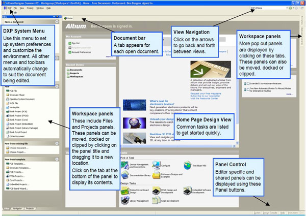
When you select All Programs > Altium Designer from the Windows Start menu to run Altium Designer, you are actually launching DXP.EXE. The DXP platform underlies Altium Designer, supporting each of the editors that you use to create your design.
The Altium Designer environment consists of two main elements:
• The main document editing area of Altium Designer, shown on the right side in Figure 1.
• The Workspace Panels. There are a number of panels in Altium Designer, the default is that some are docked on the left side of the application, some are available in pop-out mode on the right side, some are floating, and others are hidden.
Then, let's work with projects and documents
1. Create a new project
1). From the Main Menu, select File > New > Project > PCB Project. You can notice there will be a PCB Project1 behind which is "No Document Added".
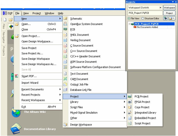
2). Back to the File, select New > Schematic.
3). Back to the File again, select New > PCB.
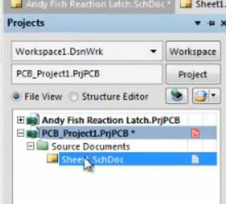
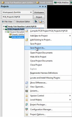
4). To save your project, just right-click PCB Project1 > Save Project As••• and you can save the project in the right place with the name you want.
2. Place schematic parts
1). Open your saved schematic file.
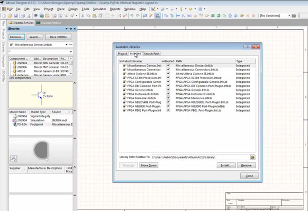
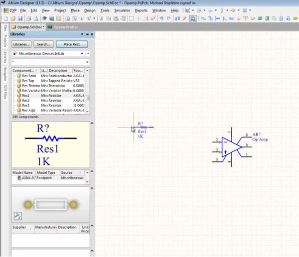
2). On the left part, click Libraries bar, select Libraries and you'll see the components you need in your design.
3). Select components and click Place *** bar to remove it onto the white paper on the right. Set them to any direction based on your needs.
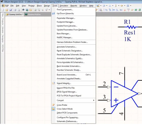
Click Tools bar, there are lots of tools for schematic modification.
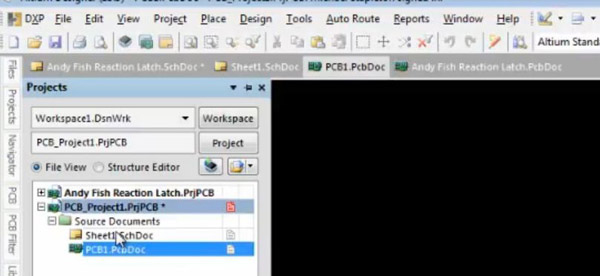
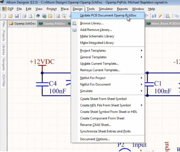
3. Update the PCB from the schematic
1). After the modification of schematic, it's time to update PCB from the schematic. Select Design > Update PCB Document***.
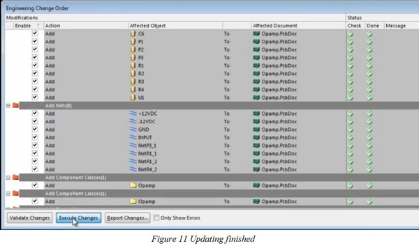
When Engineering Change Order appears, click Validate Changes and Execute Changes respectively. When ticks appear at the right side of Check and Done column, it indicates there's no problem in terms of your schematic design.
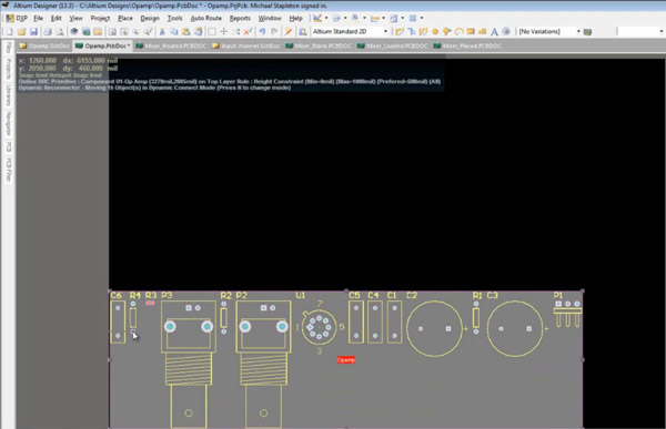
2). Here's the basic graphic of PCB design.
3). In order to use it more conveniently and make it follow the common habits of engineers, it's necessary to change this graphic into footprint view. Back to the schematic, double click any component, in the Models, select Footprint and then Add.
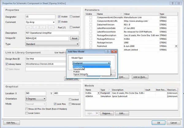
4). In the PCB Model, click Browse tab and select the right component footprint view.
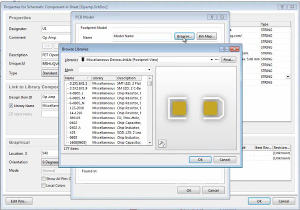
Then, the component view is like this.
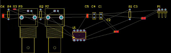
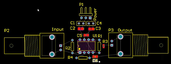
5). Then you can remove these displays according to your design requirement to make it look clear and neat.
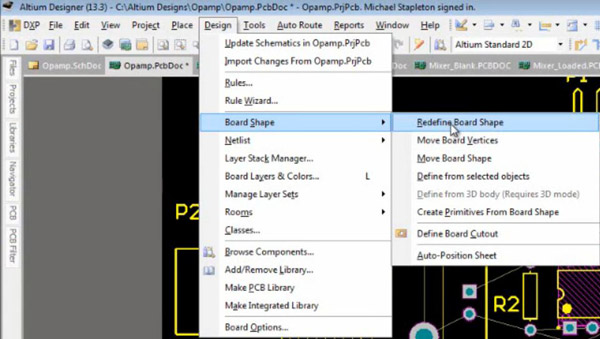
4. Board Shape and Layer
1). Circuit board design should be completed with a certain boundary so board shape must be redefined. Click Design and select Board Shape > Redefine Board Shape.
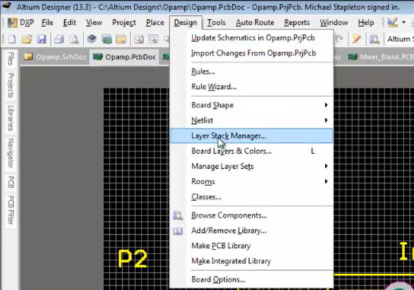
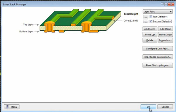
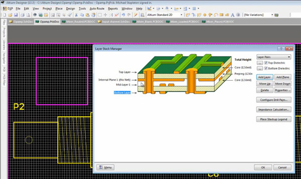
2). Usually a PCB has some layers. In the process, we have to define the specific layer for components on custom PCB. Click Design and select Layer Stack Manager.
Top Dielectric and Bottom Dielectric must be ticked if the PCB has two layers.
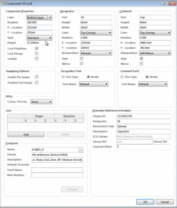
If a component is on the bottom layer of a PCB, double click the component display and set its Layer in Component Properties. Then, the layer situation of this component will be shown in the PCB design graphic.
5. Rules and Routing
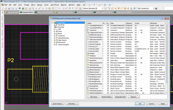
1). Click Design, select Rule... and you can choose the rules type.
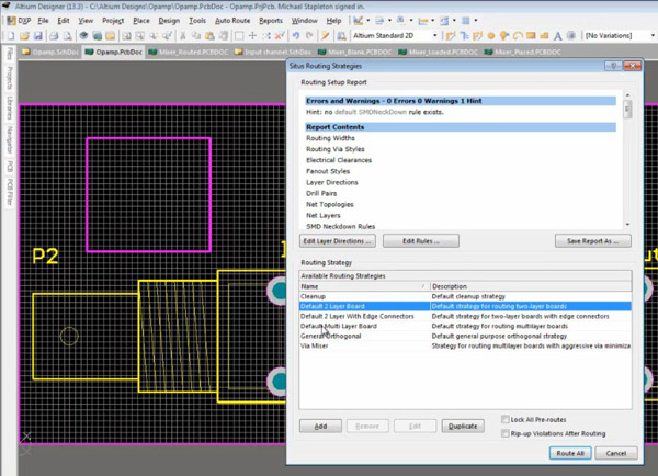
2). There's an easy way to set routs. Click Auto Route, and then select All...
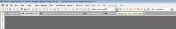
3). Auto routs is basically not the best way. There's another way to route. Click Interactively Route Connections and you can set your routes as you wish.
6. Internal planes and signal layers
Click Design and select Layer Stack Manager. Here you can click Add Layer and Add Plane to add a plane or a layer to your PCB.
7. Mounting Holes and File Generation
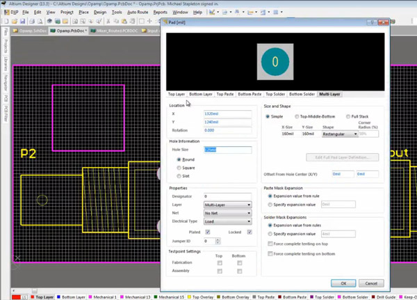
1). Click the yellow hole on the top.

2). Here, you can set the hole size, shape, net and so on.
3). You can add a string to your PCB. Click Place and select String.
You can edit the content of the string and set it placed at any layer of your PCB.
Up to now, you have finished most of your PCB design. Of course, the function realization in this tutorial is within the basic range. There are still more functions upgrading your PCBs in Altium Designer. They all depend on your practice and utilization.
Need PCB Fabrication Service? PCBCart is here to help!


