Nowadays, the transmission rate of high-performance computer interconnection network with the application of high-speed serial transmission has developed into FDR (Fourteen Data Rate, 14Gb/s), the 4th generation from the primary SDR (Single Data Rate, 2.5Gb/s), DDR (Double Data Rate, 5Gb/s) and QDR (Quad Data Rate, 10Gb/s). The design of PCB (Printed Circuit Board) with interconnection and switch board and interface cards that are essential to the formation of Internet has entered FDR high-speed and high-frequency field. Since the rising time of FDR signal has drastically reduced to the magnitude of 10ps, a series of problems concerning signal integrity has become the key features to determine the possibility of functionality implementation and reliable operation, such as attenuation, crosstalk, reflection, electromagnetic interference etc. Based on the features of FDR interconnection chips including multiple ports, multiple channels, multiple power categories and high energy consumption, multiple interconnect chips are always required to be integrated on a single interconnection board in order to increase throughput rate. On a board with limited space, on the one hand, some requirements have to be met including component layout and heat dissipation, routing with high density, long distance transmission across the back of the board and integrity of all kinds of signals. On the other hand, some elements have to be taken into consideration including PCB design period, PCB fabrication technique limitations and cost control. Therefore, it is extremely difficult for design implementation and simulation verification. Based on PCB design example of FDR interconnection and switch board, this article brings about some optimization methods in terms of substrate material selection, stack up design, routing rules and anti-interference design in order to solve the integrity problem of all kinds of signals in the process of FDR high-speed PCB design.
Attenuation Attribute and Substrate Material Selection
For FDR high-frequency signals, transmission line loss is the problem concerning signal integrity. When FDR signals are transmitted from transmitting terminal to receiving terminal along interconnection channels, because the high-frequency attenuation is much bigger than low-frequency attenuation, serious deformation has taken place to the signal waveform arriving at the receiving terminal. The deformation is mainly classified into two aspects: the voltage swing of signals has greatly decreased while bad degradation has taken place to signal rise edge. The former limits the transmission distance of signals while the latter leads to interference between codes. Transmission line loss A can be regarded as the sum of conductor loss Acond and dielectric loss Adiel as shown in Formula (1): A = Adiel + Acond.
Conductor loss refers to the loss caused by the serial resistor on copper conductor between signal path and returning path. In the situation of high frequency, skin effect makes current flow at the surface of surrounding copper conductors. With the increasing of equivalent serial resistance of copper conductors, conductor loss will rise with the increasing of frequency that is positive proportional to the square root of frequency, which is illustrated in Formula (2): 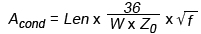 .
.
Dielectric loss refers to the loss generated by the medium of substrate material, mainly determined by the attribute of material and unrelated with geometric construction including conductor width, positive proportional to frequency, which is shown in Formula (3):  .
.
Based on Formula (2), the increase of line width is capable of reducing conductor loss. However, in the practical PCB design, the width of conductors can never be indefinitely wide as a result of limitation of spacing between pins, board, number of signal layers and impedance. The commonly-applied conductor width/spacing/width in FDR design is usually 7mil/7mil/7mil or 8mil/10mil/8mil. When the conductor width is the same, conductor loss is positive proportional to conductor length, without any relation with material. Therefore, to reduce the overall transmission loss, only dielectric loss has to be taken into consideration. Based on Formula (3), dielectric loss is proportional to dissipation factor and the application of small dissipation factors can be helpful to the reduction of dielectric loss, leading to the loss of overall transmission.
Table 1 lists the attribute parameters of three ordinary high-speed board material and loss values calculated according to Formula (1), (2) and (3) when transmission rate is 14Gb/s, conductor width 8mil and impedance 50Ω.
|
Board material parameters
|
FR4
|
Nelco4000-13SI
|
Megtron6
|
|
Df@10GHz |
0.02 |
0.008 |
0.004 |
|
Dk@10GHz |
4.10 |
3.200 |
3.600 |
|
Acond@7GHz/in |
0.24 |
0.240 |
0.240 |
|
Adiel@7GHz/in |
0.65 |
0.230 |
0.120 |
|
A@7GHz/in |
0.89 |
0.470 |
0.360 |
|
A@7GHz/30in |
27.00 |
14.000 |
11.000 |
|
Relative Cost |
1.00 |
3.500 |
8.000 |
It can be indicated that with the transmission rate to be 14Gb/s and transmission length to be 30inch, the overall transmission loss of Nelco4000-13SI is approximately 14dB while the voltage swing attenuation that typical FDR chip can withstand is in the range from 20dB to 25dB. Therefore, this type of board material can be applied in FDR interconnection switch board design with transmission distance that is less than 30inch. However, the overall transmission attenuation of FR4 is approximately 27dB and FR4 can't be applied for FDR design of long distance design but FDR interconnection interface cards with short transmission distance is allowed to select FR4 to reduce the cost. As for Megtron6 whose overall transmission attenuation is the smallest, it features the highest cost and its application in FDR leads to the increasing of system architecture fees. In conclusion, for high-frequency PCB, board material is the basis and selection of board material determines the transmission length of signals.
Layout and Stack Design
For PCB design, circuit board structure and stack have to be taken into consideration first. Usually, the pattern and shape of circuit board has been determined and the determination of stack number lies in signal frequency, circuit board pin density, PCB fabrication cost, manufacturing period and reliability requirements. FDR interconnection switch boards have high frequency and density and application of multi-layer boards is the necessary step to reduce interference. In addition, the determination of stack number is crucial.
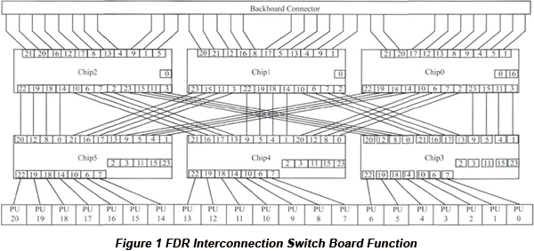
There are 24 ports on FDR interconnection chip and each port features 8 Tx channels and 8 Rx channels in the operation method of intercoupling. 6 interconnection chips and 3 downlink chips are applied by FDR interconnection board and 32 ports are accessed through backboard connector. 3 uplink chips access 21 ports through QSFP (Quad Small Form-factor Pluggable) optical fibers. Uplink chip and downlink chip are connected between each other through 4 ports, which is shown in Figure 1.
FDR features the package of BGA (Ball Grid Array) with an area of 50mmx50mm, 1157 pins and spacing of 1.0mm and P/N pins at the ports of Tx and Rx are distributed according to 3 concentric circles. Theoretically, 3 signal layers can be applied to lead all the pins at all ports out of BGA. With the following two elements considered, two signal layers can be used to access a group of pins of concentric circles.
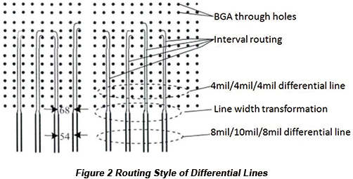
a. Owing to the limitation of spacing, the line width/spacing/width of differential lines is 4mil/4mil/4mil and it will be expanded into 8mil/10mil/8mil coming out of BGA and the distance between differential line pairs should be no less than 50mil. Therefore, a pair of differential lines has to take up a width of 2mm and 48 pairs of signals are along the edge with the biggest density. So it's difficult to implement this method.
b. Spacing between BGA pins is 1mm. If a signal layer is applied to access a group of concentric circle signals, the spacing between differential line pairs under BGA is only 14mil that is far from the required 50mil. Moreover, the max parallel routing length is only 20mm, which will generate some crosstalk.
To avoid the negative factors mentioned above, two signal layers are applied to access a group of concentric circle signals and differential signal at each signal layer has to be led out of BGA according to 50mil spacing. Therefore, at least 6 layers are required by FDR interconnection boards to make all the differential signals led out of BGA. With the connectivity and routing amount of board and enough board surface for exchange coupling capacitor considered, 8 internal signals and 22 layer stack are applied.
Crosstalk Analysis and Reduction Measures
Crosstalk is the first consideration in terms of high-speed and high-density circuit design. When voltage and current in the offensive line change, electromagnetic coupling will take place through mutual capacitance and mutual inductance between offensive line and victim line. The crosstalk flowing toward transmission terminal along victim line is called near-terminal crosstalk while the crosstalk flowing toward receiving terminal along victim line is called far-terminal crosstalk. Generally speaking, the overall noise voltage on the victim line should be controlled less than 5% of signal voltage. It's best to control the crosstalk budget of single-edge offensive line within 1% with other noise source and offensive line around two sides of victim line considered.
The key points to follow in terms of crosstalk reduction include:
a. The spacing between offensive line and victim line should be enlarged and parallel routing length should be decreased.
b. Integrated ground is applied to be the returning path of signals. According to empirical law, for the strip line of 50Ω, when the spacing is three times of line width, near-end crosstalk is approximately 0.5%. For microstrip line of 50Ω, when the spacing is three times of line width, near-end crosstalk is approximately 1%. The far-end crosstalk on strip lines or fully embedded microstrip lines is nearly zero and the far-end crosstalk polarity of microstrip transmission lines is negative with its magnitude relatively big because the influence of inductive coupling is bigger than capacitive coupling.
• Interval routing
In this design, the differential impedance of high-speed differential line is 100Ω. Based on Si9000 field solver, the line width/spacing/line width is calculated to be 8mil/10mil/8mil. The wider the line is, the smaller the attenuation is and the spacing of 10mil is to maintain the differential impedance of 100Ω. This type of differential line is applied outside BGA chip area. In order to decrease crosstalk, the spacing between two pairs of differential lines is no less than 80mil. The spacing between pins of interconnection chip in this article is 1mm and the through hole size limitation of BGA makes the line width/spacing/line width of the differential line in the BGA chip area 4mil/4mil/4mil. Although the differential impedance of this type of differential line is 100Ω as well, the lead loss is big, requiring differential line of 4mil/4mil/4mil to be transformed into 8mil/10mil/8mil as soon as it enters BGA chip area. In order to reduce crosstalk, differential line of 4mil/4mil/4mil in BGA chip area applies the way of interval routing to ensure the spacing between two pairs of differential lines more than 50mil as well, which is shown in Figure 2.
• Differential holes
Specific differential holes are set in this design for the application of exchange coupling capacitance on the connection surface layer. Ground holes have to be placed beside differential holes to provide backflow channel for returning path. Design of four ground holes features the best effect and two ground holes can be also applied when the area of board is limited. Besides, measures such as back drilling and internal pad eliminationhave should be taken to differential holes to reduce the impedance change at differential holes in order to decrease crosstalk and reflection.
• Preventing Tx and Rx from being routed in the same layer
In order to reduce crosstalk, Tx differential line should be routed in the different layer from Rx differential line. Here, Tx refers to the source terminal of differential line while Rx refers to the receiving terminal of differential line. If both of them have to be routed in the same layer, the spacing between them has to be over 5mm to ensure safety.
• 20H rule
In the PCB circuit with high frequency and high speed, RF energy is coupled by PCB power layer and ground layer and edge magnetic flux leakage is generated between power layer and ground layer. The radio RF energy can be radiated to the free space. 20H rule indicates that if there are high-speed currents on the board, there are electromagnetic fields associated with them. In the design of this article, the distance between all the routings and board edge should be at least 20 times of line width and the distance between high-speed differential holes and power plane cut-off lines is at least 5mm.
• Routing on the surface layer
In the design of high-frequency PCBs, with the relatively big far-end crosstalk between microstrip lines and strip lines considered, high-speed differential lines are prohibited on the surface layer. In the design of this article, at most 8 internal routing layers are required owing to the limitation of manufacturing craft. Moreover, the terminal arrangement limitation of interconnection chip makes it impossible for internal layers only to implement the connections of the interconnection differential lines between 6 chips inside connection board.


