OrCAD is a comprehensive PCB solution with advanced place and route technology. It provides a tiered, scalable PCB design solution that delivers advanced capabilities and highly integrated flows. Whether your designs are simple or more sophisticated with higher densities, complex rules, mixed-signal circuits, and/or standards-based interfaces, the OrCAD PCB solution has everything you need to increase your team's productivity and efficiency while reducing your overall costs and time to market.
• Proven, scalable, easy-to-use PCB editing and routing solution
• Tight application integration and a comprehensive feature set delivers a complete solution to take PCB designs from concept to production, increasing productivity and ensuring data integrity.
• Constraint Manager offers real-time validation and status of physical/spacing, samenet, region, differential pair, length rules to ensure first-time success.
• Automatic and interactive etch editing and place deliver intelligent automation to maintain user control while maximizing productivity.
• Dynamic shapes technology offers real-time copper pour plowing and healing to eliminate error-prone manual voiding and rework.
• Support for IPC-2581, STEP, and IDX brings a level of intelligence and integration that streamlines manufacturing and MCAD-ECAD flows.
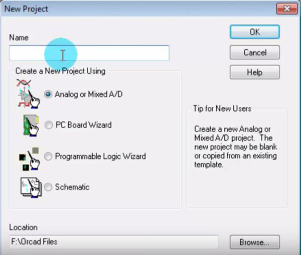
1. Click File, and select New >> Project. Create a new project by filling in a new and choose mission type in the New Project window.

2. When schematic page editor window appears, you can start to draw your schematic design on it. On the right there is a Place Part window where you can choose the suitable Libraries and then all the parts will appear in the Part list as your selection.
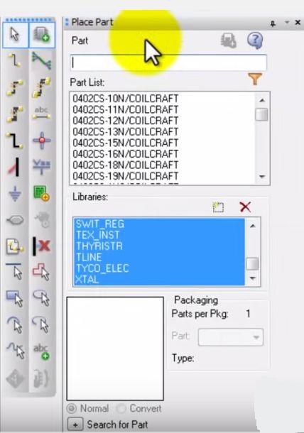
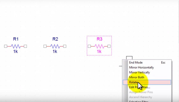
3. After choosing the right parts, you can pull them on your schematic editor window and put them at any place as you wish. Right click the part, and you can make it rotated and its direction changed.

4. On the vertical bars on the right, there are different types of editing tools including wires, power, GND and more for your selection. You can choose the right part to connect your circuit. The name of each part can be edited.

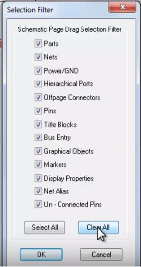
5. In the process of schematic design editing, there is a Selection Filter as long as you right click on the blank of schematic editing window. You can use selection filter to specify your selection area and objects for your edition.
6. Just like the editing in the Microsoft Word, you can cut, copy and paste your electronic parts by right clicking and choosing CutCut, Copy and Paste.
7. Choose Edit >> Properties from the menu bar, which brings up the Properties spreadsheet where you can type each name into the PCB footprint field.
8. Then it's necessary to check your design rules before PCB layout. Click on the Project Manager window and highlight your design. Select Tools >> Design Rules Check from the menu bar. Under Design Rules, select both Run Electrical Rules and Run Physical Rules. Click OK. If there is some notice of errors, return to your drawing and correct any errors, shown by green circles. Repeat until the Design Rules Check runs smoothly.
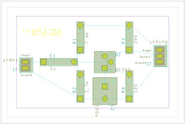
9. Now it's time to arrange the places of components. Click Place and select Manually. Then the graphic of component distribution will be displayed. You can edit the places of these components based on your innovation.
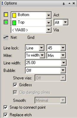
10. Routing is an important procedure in the circuit board design. Of course, the easiest way of routing is auto routing, but it isn't the ideal way. In OrCAD, before routing, you must make sure that no objects are selected. Then click Route >> Connect on the menu bar. And you have to set the features of routing including layers, pins, vias and so on.

11. The machining files required for PCB manufacturing are generated by the "post processor". From options menu choose Post Processing. In the spreadsheet, select the layers you need to manufacture. You need at least the routing layers you have used and the drill information. Choose Auto >> Post Process to generate the files. The files generated by the post processor are the only ones needed for the PCB plant to make the board.
Up to now, the steps this passage has shown you are just within the quick start range. The functions and capacity of OrCAD are far more than the steps above. You are encouraged to make full use of this software and we believe you'll obtain and discover more.

