At present, the fast development of Internet technology witnesses the massive application of email, online payment and personal communication. Under this background, information security has been a critical research theme around the world. PKI (Public Key Infrastructure) technology provides security service by using public key theory and technology. PCIE (Peripheral Component Interface Express) technology has received wide applications in high-speed devices as the third generation I/O bus standard applying serial data transmission and point-to-point interconnection technology. In the field of digital system design, relatively high clock frequency leads to some problems in perspectives of signal integrity, power integrity and crosstalk and traditional PCB design fails to meet the requirement of system stability.
This article offers a PCB design scheme on high-speed password card based on PCIE according to the benefits of PCIE high-speed serial transmission.
Overall Design Scheme
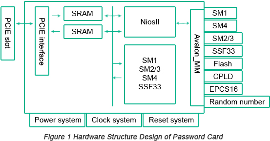
FPGA chip EP4CGX50CF23C6N belonging to Cyclone IV GX designed by Altera is applied in this design, integrating PCIE IP hardcore module and implementing 4 high-speed data transmission password card design. Four types of chips, chip 1, chip 2, chip 3 and chip 4, are capable of respectively implementing algorithms of SM1, SM2/SM3, SM4 and SSF33 and implementing functionalities of password card initialization, secret key administration, backup and recovery and authority management. Password cards are applied in PCs, connected with main board in PCs through PCIE slot and controlled by PCs. IP hardcore in FPGA is applied to implement PCIE, leading to the communication between PCIE core and SRAM cache and control module. As the control center, NiosII implements the function of password card software. Meanwhile, additional password chip implements the communication between each interface module and password card. The hardware structure design of password card is illustrated in Figure 1 below.

High-Speed PCB Design
• Stackup and layout
Stackup design is the most significant problem that should be taken into account and reasonable stackup design can inhibit EMI (Elcetromagnetic Interference) radiation, making transient voltage on power plane or ground layer be as small as possible and shielding the electromagnetic field of signal and power. Generally, multi-layer board and multiple powers are applied in high-speed digital circuit design. PCB stacking design is implemented based on comprehensive elements including circuit clock frequency, PCB fabrication cost, pin density, manufacturing period and reliability. Moreover, layers of multi-layer board should be maintained symmetrical and the number of boards should be an even number since asymmetrical stacking design will cause warpage of boards. The password card designed in this article is connected with PC through PCIE slot and the size and shape of the circuit board is fixed with the height approximately 67mm and length approximately 174mm, configuring PCIE X4 interface pin at the bottom. As a result of the high component density and thick routing, the number of PCB layers is picked up as 6 layers with distribution of signal layer, power layer, signal layer, power layer, ground layer, signal layer. This design containing 3 signal layers, 1 ground layer and 2 power layers, providing the environment required by signal integrity.
After the determination of PCB stacking, component groups and layout should be implemented. First, position of components has to be programmed in accordance with the dimension and pattern of PCB, taking line-connection, functional partitioning and trim and beauty between components into consideration. Then, components have to be reasonably distributed according to different grades of component voltage to make voltage wires as short as possible, which is capable of reducing the interference of power noise and increasing stability of power. Chip placement should pay attention to the relationship between its auxiliary circuit and its chip and to placement of crystal oscillator behind clock pins. High-noise components should be avoided being placed around crystal oscillator and should be near its driving components. Furthermore, the placement of each chip power and signal pins has to be considered with their positions and direction adjusted based on the connected lines. Because the ratio of length and width of password card is more than 2:1 with the positions of PCIE slot, loading holes and indicating LED fixed, component layout for fixed components has to be considered first in component layout. In addition, as a result of the large number of connecting lines between component and FPGA, the component layout should be implemented with FPGA as a center prior to positions of other components so that the top and bottom room of PCB can be effectively used in order to leave enough space between components and components and positioning holes.
• Power design
In high-speed circuit board design, design of power system is directly related with the success of the whole system. Noise generated by power and ground should be reduced to the minimum in order to ensure the reliability of products. The application of power distribution scheme in the method of layers refers to the fact that power is distributed through the metal on the whole layer, decreasing power impedance and noise and increasing reliability. Because multiple powers are concerned by PCB, multi-power layer design should be applied, capable of eliminating public impedance coupling interference as a noise loop. The application of decoupling capacitance is capable of solving the problem of power integrity since capacitor can be only placed on the bottom layer or top layer of PCB, based on which wires connecting decoupling capacitors should be short and wide. According to chip material, the current passing through power lines can be calculated and width of leads can be determined. The wider leads are, the more current they can carry. The experimental formula is illustrated as: W(line width: mm) ≥ L(mm/A) x I(current: A)
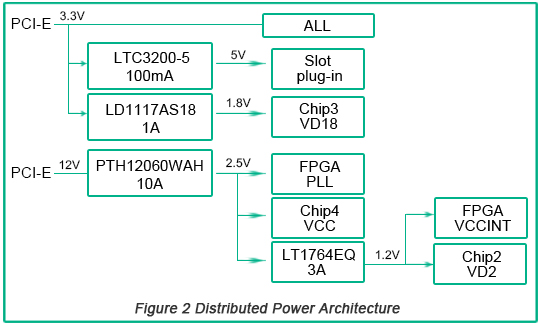
Multiple powers on PCB obtain one or two types of power from power board using back board and the power is then converted into other power required by components. The conversion of power is divided into two architectures: centralized power architecture and distributed power architecture. The former refers to power is supplied by an independent power and then converted into all kinds of required powers while the latter refers to multi-grade power conversion. Because centralized power architecture features disadvantages of high cost and large PCB area, distributed power architecture is applied in this design. Cryptographical card concerns 6 powers, including 12V, 3.3V, 5V, 2.5V, 1.2V and 1.8V. This design starts with the participation of 3.3V and 12V power in PCIE slot and then 3.3V power is capable of generating 5V power and 1.8V power through voltage conversion chip, supplying power for plug-in and chip 3. Next, 12V power is converted into 2.5V power to supply power for FPGA and chip 4. Finally, 2.5V power is converted into 1.2V power to supply power for FPGA and chip 2. The distributed power architecture of cryptographical card is shown in Figure 2 below.

• Through-hole design
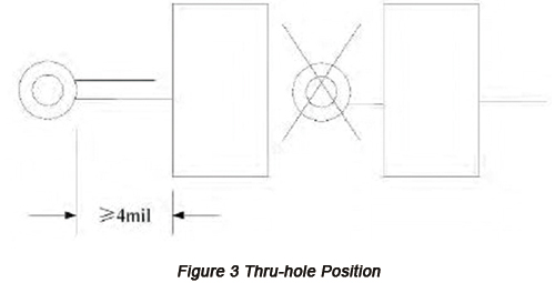
In the process of design layout for multi-layer PCBs with high density, through holes should be applied, transmitting signal from one layer to another layer to provide electric communication between layers. Position design of through holes has to be implemented with much care. Through holes mustn't be placed on pad and one printed line can be applied for connection, otherwise leading to problems such as tombstone and insufficient solder. Soldermask has to be coated on through hole pad with distance set to be 4 mil and through holes mustn't be placed at the center of pad for chip components on soldering side. The position of thru-holes is illustrated in Figure 3 below.

Moreover, thru-hole position mustn't be too near to goldfinger whose plug-in side should contain chamfer. In order to make circuit boards plugged in PCIE slot, chamfer of (1~1.5)x45° can be designed on two side edges of plug-in board.
• High-speed signal routing
In the process of routing, distribution has to be adjusted reasonably to make connecting lines the minimum so that crosstalk can be reduced. In the process of high-speed digital signal routing, signal layer near multi-power layer routing should be far away from power reference surface in order to avoid the generation of returning path by signal current.
Since high-speed circuit clock signal frequency is relatively high, the jitter, drifting and deformation greatly influence the system so that high-speed PCB design requires small signal wave interference. Therefore, the problem of clock distribution and routing should be firstly considered. Routing has to be implemented on high-speed clock signals and the routing of main clock signal lines has to be as short as possible, straight and free from thru-holes and power part in order to prevent the crosstalk between clock and power. When multiple clocks with different frequencies are applied on the same PCB, two clock lines with different frequencies mustn't be maintained parallel. However, for multiple components using clock signals with the same frequency, network can be distributed by spider type, tree type and branch type.
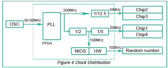
In high-speed cryptographical card, FPGA obtains 66.66MHz clock through the crystal oscillator on PCB. After looping with intrinsic locks inside FPGA, 200MHz basic clock is generated as the interface for chip 2 and chip 3 to operate clock. Then 100MHz clock is provided after intrinsic frequency dividing circuit as NiosII softcore and the working clock of hardware circuit inside FPGA. The divided frequency 16MHz is the working clock for chip 2 and chip 3 while the divided frequency 20MHz is the working clock for chip 1 and chip 4. Clock distribution is displayed in Figure 4 below.

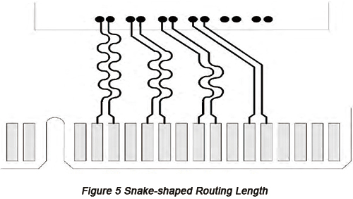
High-speed signal transmission between PCIE slot and PC is implemented by high-speed cryptographical card in the way of differential pair routing to avoid problems concerning signal integrity. Generally speaking, grounding wires aren't placed between differential pair signals, otherwise coupling effect between differential pair signals will be destroyed. After the routing of differential pair signals, copper is placed around PCB high-speed signals with spare space fully filled with grounding wires to increase circuit's EMI capability. The key of PCB routing is to maintain the symmetry of differential pairs. If the length of differential pairs isn't compatible, the accuracy of data reading and writing will be affected with the data transmission rate decreased. To ensure the system's validity of data reading within the same period, the delay difference between differential signals has to be maintained within an allowed category and the routing length must be strictly the same. Therefore, snake-shaped routing can be applied to solve this problem by adjusting time delay. In this design, communication is implemented by PC through PCIE and cryptographical card and the transmission and receiving of high-speed signals are implemented by differential pair signals with the length of PCB routing controlled within 25mil. The matching diagram of snake-shaped routing length is illustrated in Figure 5.
