With constant progress of electronic technologies, increasing high frequency of clock in digital system, increasingly short rising edge time, PCB system has become a system structure with high performance, far more than just a platform supporting components. From the perspective of electric performance, the interconnection between high-speed signals is no longer expedite or transparent and the influence of interconnection between leads on high-speed PCB and board plane properties can't be neglected any longer. Successfully deal with problems of signal integrity including reflection, crosstalk, delay, calling & impedance matching caused by high-speed signal interconnection and ensure the quality of signal transmission determines the success of the design.
Basic Theory of PCB Signal Integrity
• High-speed circuit and its determination principle
The defining term of high-speed circuit comes primarily in two versions. On the one hand, in a circuit, when the delay of digital signals on transmission lines is more than 20% of rising edge time, this circuit can be regarded as a high-speed circuit. On the other hand, in a circuit, when the frequency of digital analogy circuit reaches or exceeds by 45MHz to 50MHz, the circuit is regarded as high-speed circuit.
Basically, if L (length of leads) is more than Tr, the circuit is regarded as high-speed circuit; if L is less than Tr, the circuit is regarded as low-speed circuit. Here, Tr refers to pulse rising edge time.
• Signal transmission speed and pulse rising edge time
The transmission speed rate of signal in the air is 3 x 10 8m/s; the dielectric constant of FR4 that is the material of PCB is displayed as εr that is 4. Signal transmission speed rate in PCB can be calculated using Formula  .
.
Vp is equal to 15cm/ns that is approximately 6inch/ns. Pulse rising edge time Tr=1/(10 x fclk) and the rising edge time of 100MHz signal is 1ns. When the delay of signals on PCB routing is more than 20% of rising edge time, obvious calling will take place on signals. For sqaure wave whose rising time is 1ns (100MHz), when the routing length of PCB is more than 0.2ns x 6=1.2inch, serious calling will take place on signals. Therefore, the critical length is 1.2inch (approximately 3cm).
• Characteristic impedance
Characteristic impedance is an important parameter in impedance matching that influences reflection, calling, upper shoot and under shoot and directly relates with integrity of high-speed signal transmission, which is very important in high-speed design.
Signals transmit along transmission lines, whose ratio between voltage and current is regarded as transient impedance. The transient impedance on transimission lines is calculated by Formula 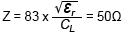 . In this formula, Cl refers to capacity per each unit length whose unit is pF/inch (it is usually 3.3pF/inch). When the transient impedance along transmission lines is a constant value, this value is regarded as the characteristic impedance on transmission lines. For microstrip lines and strip lines on PCB, their characteristic impedance can be figured out by transmission line design tool Polar Si9000, which is shown in Figure 1.

Elements Influencing Signal Integrity and Solutions
• Impedance matching
Impedance matching is required in high-speed circuit design in order to ensure fast and correct data transmission. Data accumulation system is generally composed by sensor, signal conditioning instrument, AD data accumulation chip, FPGA and SDRAM, as is shown in Figure 2.

AD9649 is applied as AD chip with a 1.8V power supply and parallel sample by 14 bit data line. The frequency of sample is set to be 20M. PCI9054 is picked up as PCI interface chip, supporting DMA data transmission. 93LC66B is picked up as PCI configured chip. HY57V561620FTP-H is applied as data storage, consisting of 4 BANKs each of which has memory space of 4M x 16bit, 13-row address lines and 9-collum address lines. EP1C6F256C8 is chosen by FPGA with a termianl voltage of 3.3V and core voltage of 1.5V. The width of PCI bus is 32 bit with 33MHz clock picked up as the writing and reading clock and the max speed of wiring and reading reaches 132MByte per second, capable of supporting high-speed transmission of accumulated data.
The following elements should be taken into consideration in the process of designing PCBs:
a. As a mixing part of digital and analog, AD is one of the key points in PCB design. Owing to the high frequency of digital part, analog part is quite sensitive to interference. If suitable processing isn't implemented, digital signals will tend to interfere analog signals so that EMI problems will take place. The correct principles designers follow should be: first, digital ground and analog ground should be divided on PCB with mixed signals; second, analog and digital electronic components are classified with analog ground distributed in analog area and digital ground distributed in digital area; third, analog ground and digital ground are connected with magnetic beads around region segmentation. These measures is capable of implementing the separation between digital ground and analog ground.
b. SDRAM is applied in data accumulation system and the manual clearly indicates that data lines that are connected with FPGA have to be configured with impedance matching of 50Ω in order to ensure the high-speed transmission, which is shown in Figure 3.

After FPGA writes accumulated data into SDRAM, refreshing has to be constantly carried out in order to maintain data and refresh period of each row has to be faster than 64 milliseconds.
Steps of impedance matching by Polar Si9000 software are displayed as the following:
a. High-speed signal lines should cross the top surface of PCB and holes should be avoided as much as possible. Microstrip line structure model is picked up in the software, as is shown in Figure 4.

Impedance matching of 50Ω is generally carried out at single-terminal routing and impedance matching of 90Ω is generally carried out at differential routing (such as USB2.0 D+, D-).
b. Necessary impedance matching value and specific values of PCB fabrication technique are filled on software interface with parameters including dielectric thickness, dielectric constant of PCB material, copper foil thickness, green oil thickness and dielectric constant of green oil.
|
Item
|
Description
|
Reference and calculated value
|
|
H1 |
Dielectric thickness (PP or board material) |
3.5-8.5mil |
|
Er1 |
Dielectric constant of board material |
4-4.6 |
|
W1 |
Signal routing width |
Based on impedance value |
|
C1 |
Thickness of green iol of substrate material |
0.8mil |
|
C2 |
Thickness og green oil on copper |
0.5mil |
|
CEr |
Dielectric constant of green oil |
3.3 |
|
Zo |
Impedance value to be matched |
Single terminal: 50Ω
Differential: 90Ω |
Specific parameters of fabrication technique can be known through communication with PCB manufacturer so that width of leads can be figured out. For differential microstrip lines, distance between leads (S1) also should be figured out.
c. If the calculated width of leads is relatively big and PCB routing fails to be completed, more communication has to be made with PCB manufacturers to adjust parameters in fabrication technique with design requirement met.
• Crosstalk
Crosstalk refers to unexpected voltage noise interference on adjacent transmission lines as a result of electromagnetic coupling when signals are being transmitted on transmission lines. Too much crosstalk may lead to false triggering of circuit so that system fails to normally work. Crosstalk is generated by electromagnetic coupling and coupling is divided into capacitive coupling and inductive coupling. The former is actually electromagnetic interference led by inductive current that is caused as a result of voltage change at interference source while the latter is actually electromagnetic interference led by inductive voltage that is caused as a result of current change at interference source. As the state of interference source changes, a series of interference pulse will be generated on interfered objects, which is very common in high-speed system.
Measures to deal with crosstalk are displayed as the following:
a. Orthogonality should be kept on routing directions between adjacent planes. The same direction should be avoided in adjacent planes with different signal lines in order to reduce crosstalk. Especially when signal speed rate is relatively high, ground should be considered to separate routing planes and signal lines should be separated by ground signal lines.
b. In order to reduce crosstalk between lines, spacing between lines should be large enough. When distance between centers of lines is no less than three times of line width, 70% of electrical field can be stopped from mutual interference, which is 3W principle.
c. In the situation where high-speed signal lines meet the requirement, matching can be accessed to joining terminal to reduce or eliminate reflection and to decrease crosstalk.
Application of Signal Integrity Design Method
In the process of PCB design, a lot of design rules have been summarized based on signal integrity theory. With reference of these PCB design rules, signal integrity can be obtained better. In the process of PCB design, design information has to be known in detail, including:
a. Component layout position, whether there are special requirments on components with large power and heat dissipation on chip components.
b. Classification of signals, speed rate, transmission direction and impedance matching requirement.
c. Signal driving capacity, key signal and protection measures.
d. Types of power, ground, noise limit requirement of power and ground, setting of power plane and ground plane and division.
e. Type and speed rate of clock lines, source of clock lines, direction, delay requirement of clock and maximum routing requirement.
Helpful Resources:
• 3 Routing Techniques on PCB High-speed Signal Circuit Design
• Suppression Method of Signal Reflection in High-Speed PCB Layout
• Signal Integrity Analysis and PCB Design on High-Speed Digital-Analog Mixed Circuit
• Impedance Control of Vias and Its Influence on Signal Integrity in PCB Design
• Full Feature PCB Manufacturing Service from PCBCart - Multiple Value-added options
• Advanced PCB Assembly Service from PCBCart - Start from 1 piece


