PCB successfully added to your shopping cart
PCB Layout Influence of Electronic Product EMC Performance
• Influence of Common Code Interference to PCB Inner Signal
Printed Circuit Board (PCB) inner printed lines feature parasitic parameters relative to reference ground board and when function signals are being transmitted inside PCB, the same equipotential node in the same network in the circuit isn't equipotential any longer. The current i inside PCB starts from source end, passes a series of carriers returns to the signal source, forming a signal. What's more, i tends to flow along the path with low impedance so that i usually keeps unchangeable with the stability of impedance.
Figure 1 indicates the process when common mode interference is transformed to differential mode interference inside PCB. id refers to the differential mode current inside PCB flow while icom refers to the common mode current that either starts from outside PCB and flows into PCB through reference ground board or starts from the inside of PCB and returns to inside of PCB through reference ground board. High-frequency icom has two paths: the first is from point A to point B inside PCB starting from GND; the second is from point A to point B starting from port S1 to PCB inside by capacitance C. Ground impedance ZAB leads to the generation of ΔuAB, so when normal signal is passed to IC2, deformation will take place to signal and common mode interference is transformed into differential mode interference, which produces influence to normal signal based on the formula that is u2=u1-ΔuAB.
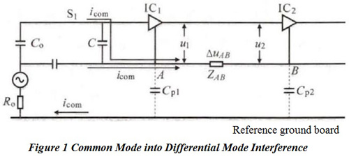
Therefore, as soon as icom enters the inside of PCB through I/O port or space radiation, differential mode filter capacitance on signal lines of PCB can only press interference bypass to GND. The prerequisite of this result is that GND is regarded as low impedance for signal backflow and current always flows towards the direction of low impedance.
• Key of EMC Design Implementation: Ground Impedance in PCB
The reason for the generation of EMC by high-frequency signals lies in that signal reference level GND fails to maintain its feature of low impedance. With the increase of impedance ZGND of reference level, the quality of signal transmission decreases as well. In order to solve the problem of high-frequency interference, common methods are used in EMC design such as filter, ground and shield that are closely connected to "ground".
Filter can be regarded as capacitor to ground, with two structures one of which is to make X capacitor connected to signal reference ground and the other of which is to make signal connected to metal shell by Y capacitor or different ground connection inside PCB. Shield can be regarded as the result of PCB ground's expansion to space. The purpose of filter or shield is to make high-frequency common mode interference pass the bypass with low impedance in order to avoid flowing into normal operation signal. Similarly, all these methods won't work unless ground has low impedance.
Figure 2 indicates the effect of ground impedance to circuit filter. icom flows according to the sequence of IC1→IC2→IC1 and when it flows to point P, icom will flow into branch circuits of IC1 and C1 through which it flows from point A to B. If the impedance between point A and B, that is ZAB, is far less than the impedance between point P and IC1. At this moment, icom flows from point P to A, IC1 filter can be realized. When icom flows to point B, branch circuits will occur that are B→C and B→Q. If PCB layout isn't well controlled, the impedance between point B and C, that is ZBC, ZBC>>ZC2+ZQ. ZQ refers to the impedance between point Q and IC2. icom flows backward to IC2 input port through C2 when capacitance that was originally used solely for IC2 plays a role in signal invasion interference.
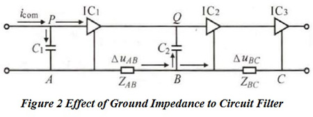
In order to make reference level with low impedance, it is usually designed to be a surface. Generally speaking, conductor whose length-width ratio is less than 5 can be regarded as low impedance in the field of engineering. The impedance of printed lines isn't determined by its degree of length or thickness. In the traditional PCB design principles, analog circuit single point grounding is massively recommended so PCB layout principle of digital circuit multiple points grounding and digital module circuit mixture grounding are no longer workable for dealing with EMC problems.
Since all backflows of all signals must be ensured to feature an integrated ground with low impedance, 4-layer or multi-layer boards with integrated ground plane are capable of meeting the requirement while low-cost single boards aren't. When a double-layer board has to be used based on the limitation of cost, a relatively integrated ground plane should be designed for signals inside PCB. In the practical application, PCB ground impedance is influenced both by its shape and by signal wire through holes, crack and slotting. Figure 3a and 3b respectively display bad and excellent low impedance ground plane design.
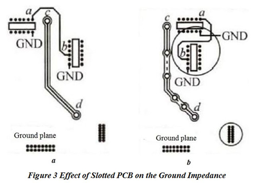
In this figure, all the components are at the front side of PCB while ground plane is at the back. Chips are connected through printed lines ab at the front side and cd is printed lines at the back side. Under the pressure of high-frequency common mode interference by the outside, the slotting formed by cd will lead to the increasing of ZGND of printed lines backflow. ZGND fluctuates in the process of signal transmission, leading to low quality of signal. Therefore, layers of printed lines between cd can be exchanged over and over again through holes in the process of PCB layout design so that ZGND will be decreased. Besides, two ICS with sensitive signals can be arranged together so as to make GND become a relatively integrated ground plane locally to ensure signal won't be interfered in the process of signal transmission. Pay attention that through holes can't be arranged with much density, otherwise crack on ground plane will be caused as well, leading to the escalation of ZGND.
Stacking Design of PCBs
EMC design is best for 4-layer PCBs. From the perspective of EMS, either metal shell or metal shell shield of locally sensitive circuits is capable of solving interference problems. From the perspective of EMI, sometimes 4-layer boards fail to meet the requirement of radiation emission limitation and number of layers should be increased since multilayer boards can make signals with high du/dt and di/dt ensure smaller signal loop area in the process of transmission, providing backflow with low impedance for high-speed signals.
The basic principle of PCB stacking design is to arrange high-speed signal layer and power plane adjacent to ground plane. Figure 4 shows the stacking design of 4-layer and 6-layer boards. S1 in Figure 4a refers to high-speed signal layer while Figure 4b, 4c and 4d are three ordinary 6-layer PCB design.
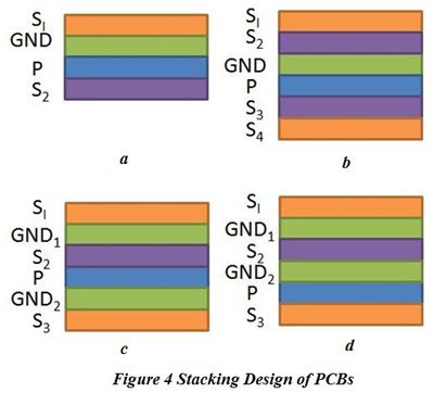
Among the 3 6-layer PCB design, design b is the worst and S2 layer should be high-speed signal layer. S2 layer in design c and d is high-speed signal layer. Design c is the best because each signal layer is closely adjacent to ground plane in order to ensure the shortest signal backflow path and S2 and P layers are shielded by GND1 and GND2. Compared with design c, S3 in design d is far from GND layer and P can only reach the single-side effect instead of double-side effect caused by design c.
Equivalent Antenna in PCBs
The fundamental function of antenna is to radiate and receive wireless radio wave. In the process of radiation, high-frequency current can be transformed into electromagnetic wave; in the process of receiving, electromagnetic wave is transformed into high-frequency current. The radiation in EMC field mainly refers to far-field radiation. The formation of antenna depends on two basic conditions: RF signal source and certain length of conductors connected to RF signal source. In the field of engineering, it's believed that antenna effect will come up when the length of conductor in accordance with the formula that is l=λ/20. When l=(λ/4)n, antenna effect is the biggest with n as natural number.
When signal is being transmitted inside PCB, inner loop has the same effect with loop antenna. The larger the loop area is, the more the antenna effect will be. Strict PCB loop control can effectively stop differential mode interference, which is feasible in practice. However, increasing length of printed lines will cause obvious rod antenna effect so length of interconnect signals should be cut down as much as possible in the process of PCB layout.
When relatively high ZGND takes place on the backflow path of high du/dt signals transmitted inside PCB, common mode driver source ucom will take place with icom flowing past ZGND, together with connected printed lines or I/O stables, which can radiate outside.
If PCBs are relatively small in size, inner printed lines can't reach antenna radiation requirement because of limitation of length. Under this condition, I/O cable can be regarded as the expansion of printed lines, radiation requirement can be met. Even if no direct connection to I/O stable exists, crosstalk coupling should be stopped between I/O cables.
Crosstalk inside PCB and Its Remedies
• Coupling between PCB printed lines and reference ground
Since EMC mainly discusses high-frequency common mode signals, distribution parameters can neither be avoided inside and outside PCB. Capacitive coupling occurs between PCB and reference ground whose distributed capacitance is composed by plate capacitance and natural capacitance within the smallest space. Plate capacitance is directly proportional to the size of PCB and indirectly proportional to the distance between PCB and ground. Natural capacitance within the smallest space is directly proportional to equivalent diameter of printed lines inside PCB. Therefore, no matter where PCB is placed, even far from the ground in infinity, distributed capacitance always exists between inside printed lines and ground. In a PCB, the distributed capacitance of a relatively integrated GND plane to reference ground board is approximately 10pF and the distributed capacitance of inside printed lines to reference ground board is approximately in the range from 0.001pF to 0.1pF or lower. The distributed capacitance of printed lines in the center of PCB is much lower than that of printed lines at the edge of PCB.
• Coupling inside PCB
a. Theory of coupling inside PCB and its influence to signal
Coupling inside PCB consists of capacitive coupling and inductive coupling whose theory is displayed in Figure 5.
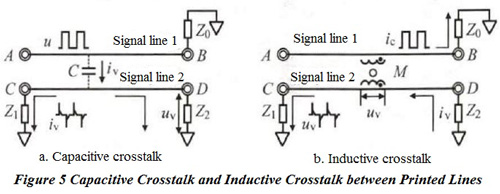
In this figure, both AB and CD are parallel printed lines with small space between two lines. Z0 refers to the carrier of signal line 1 while Z1 and Z2 refer to respectively carriers of signal line 2. In Figure 5a, when the signal peak voltage on the printed line AB is u, signal rising time is Δt, and angular frequency is ω, the voltage of Z2 will be uv=[Z1Z2/(Z1+Z2)]cΔu/Δt. Although c has a very low value, the value of Δu/dt can be very high and their product can't be avoided. In Figure 5b, when the peak current of signal on AB is Ic, signal rising time is Δt, and angular frequency is ω, the mutual inductance m between 2 printed lines will pass through CD on which induce voltage is uv=mωic. Although the value of m is so small, signal frequency may be increased. Therefore, their product can't be avoided.
As a result, both capacitive coupling and inductive coupling are related with two printed lines' distributed parameter c or m. During PCB layout, values of c and m can be reduced by increasing distance between parallel lines. In practical circuit, capacitive coupling accounts for most of digital circuit and when PCB plane isn't smooth or slotting or crack exist, inductive crosstalk will have more influence than capacitive crosstalk. However, when the area of PCB is limited, crosstalk can't be dealt with solely by enlarging the distance between parallel lines. In order to maintain the smallest distributed parameters between two adjacent parallel lines, integrated plane design should be arranged in the projective area and it's best to have ground layers at the top and bottom.
b. Influence of shield ground wire to reduce crosstalk
The degree of crosstalk is determined by lots of elements such as signal frequency, signal rising edge time, distance between signal lines, driving port and electric features of receiving port and number of PCB layers. Crosstalk can be decreased by setting integrated ground plane under printed lines and shield ground wire can be added between signals.
In the process of PCB layout, two aspects can be beneficial to stop crosstalk. Firstly, sensitive inner circuit and outer circuit should be stopped. Secondly, crosstalk between inner circuit or noise circuit and other signals should be stopped. In the practical PCB layout, detailed test should be carried out in the same layer or between different layers in PCB to detect whether crosstalk risk exists or not.
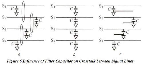
During the procedure of PCB layout, some signal lines with the same attribute should follow the routing of same time and same direction with density. If the limitation of PCB space leads to the fact that filter components can't be placed on the same line, crosstalk between signals tends to be aroused. This situation is indicated in Figure 6 below.
c. Influence of shield ground wire to edge effect
When highly sensitive signal lines or signal lines with high du/dt, di/dt are arranged along PCB edge, they will suffer more EMC risk than those arranged in the center of PCB. It's easier for edge signal lines to make receiving high-frequency interference or outer radiation by larger parasitic capacitance.
Under the limitation of the area of PCB, it's extremely difficult to layout PCB according to 20H principles in the design file. "Packet" can be used to reduce interference and outer radiation. Packet lines don't need to meet specific requirements such as thickness and shape. Usually when a signal line is too close to PCB edge to plate copper, a ground line in the range of 7 to 10mils can be added as a shield.
d. Mutual interference between digital and analog circuits
When a PCB holds high-speed digital circuit and low-level analog signals, crosstalk is usually generated to analog signals by digital noise under bad PCB layout. The mutual interference between digital and analog circuits is caused by the following reasons. Firstly, crosstalk noise is caused by parasitic capacitance and parasitic inductance. Secondly, the bad decoupling of power ripple and digital chip power will lead to power noise. Thirdly, ground impedance and system ground place cause noise. The problem of noise should be dealt with in the order of power, signal and ground.
Helpful Resources:
• The Most Comprehensive Introduction of EMI and EMC Automated Tools
• Ensuring First-Time Success in PCB EMC Design
• PCB Partitioning Design Rules for EMC Improvement
• PCB Design for Radio Frequency Circuit and Electromagnetic Compatibility
• Three Design Considerations Ensuring EMC of Laptop PCB
• Full Feature PCB Manufacturing Service from PCBCart - Multiple Value-added options
• Advanced PCB Assembly Service from PCBCart - Start from 1 piece


