With the improvement of technology and people's living level, people's requirement on electronic products have moved towards lightness, thinness, miniature, high performance and multiple functions so that miniature and integrity of electronic products have become the main direction of their development. In order to increase the density level of components, lots of single-side and double-side circuit boards primarily manifest surface mount components (SMCs) or surface mount devices (SMDs). However, in terms of intrinsic intensity, reliability and applicability, PIP components still hold more advantages than SMCs and SMDs in some cases, especially for edge connectors. For example, in double-side SMT (Surface Mount Technology) boards featuring mixed assembly with few PIP components on the top, application of PIP technology is helpful to process reduction and cost control. PIP technology is a printing method by template, that is, some amount of solder paste is printed on the surface of SMCs and on through holes and pads of through-hole mounted components. After the completion of mounting, soldering is completed after high-temperature oven.
Compared with traditional technology, PIP technology has the following advantages:
a. PCB fabrication and technology process is simplified owing to the absence of wave soldering.
b. Workshop space is saved due to fewer applications of needed equipment, material and workers.
c. PCB manufacturing cost is decreased while production cycle is shortened.
d. High defect rate caused by wave soldering can be avoided so that first pass yield can be improved.
e. One or more heat treatment steps can be omitted so that PCB solderability and component reliability will rise.
f. Thru-hole reflow (THR) technology is capable of reducing the amount of flux, avoiding the contamination of flux on PCB caused by wave soldering.
Properties of OSP Surface Finish
As a transparent organic material surface finish of PCB, on the one hand, OSP holds an extremely high requirement for PCB storage and short craft time while generally after one-time high-temperature soldering, the organic protection film on the surface of PCB will be destroyed so that anti-oxidation capacity will be lost, easily leading to difficulties of second-time reflow soldering. On the other hand, PCBs with OSP surface finish have worse solder paste flowability and copper tends to be exposed on solder joints, which influences reliability of solder joints. In addition, the appearance of tin coating fails to comply with IPC3 standard. Therefore, generally, PCBs with OSP surface finish are seldom applied in products with PIP technology. Nevertheless, most companies still love using PCBs with OSP surface finish since boards have excellent evenness and PCBs with OSP hold relatively stable fabrication technology with a low cost, which is difficult for other types of surface finish to obtain.
Requirement on Components
• Components should adhere to the requirement of reflow in the aspect of temperature withstanding capacity.
For example, lead-free process components should withstand the temperature of more than 260°C for more than 10 seconds. Professional PCB manufacturers should have the capabilities to process lead-free surface finish. Take PCBCart, a custom PCB assembly manufacturer for example, is very excellent in lead-free processing. For experiment purpose, we'll only apply lead-free craft in this article.
• Tin paste is required to be coated on top of vias for THR.
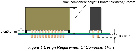
To make this process applicable, the distance between components and board should be 0.3mm-0.7mm when applying PIP technology. Under the same conditions (printing parameter, pad and aperture diameter design etc.), pins of PCB components with immersion gold and other types of surface finish is 1.5mm thicker than board thickness and tin coating of solder joints at the bottom is capable of meeting the requirement of IPC3. However, copper leakage tends to take place to solder joints on PCBs with OSP and the appearance fails to comply with IPC3 standard.
After multiple times of verification, tin coating receives better effect when pins of components on PCB with OSP are longer than board thickness by 0.5mm to 1.0mm, which is shown in Figure 1 below.

In order to stop component pin from pushing out tin paste inside aperture with tin amount inside aperture insufficient, sharp corner or cone processing has to be carried out on component pins.
• Component material package requirement should be the same as that of SMT.
Components have to adhere to the requirement of automatic mounting of SMT equipment. The requirement covers aspects of component height, component shape, spacing between component pins, etc.
Requirement on Pad Design
PIP technology is applied to PCBs with OSP surface finish. Component layout requirement should be largely compatible with PCBs covered by other types of surface finish. General principle is that small components are placed at bottom side while large components are placed at the top side in accordance with the requirement of double-side reflow soldering. Components mustn't be placed within 2mm around PIP components; if multiple PIP components exist, to stop interference caused during automatic mounting, the distance between adjacent PIP components should be 10mm at least.
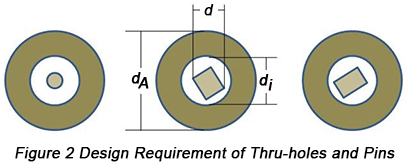
To avoid generation of tin connection between adjacent pins or between pads which may cause insufficient tin inside aperture or short circuit, distance between adjacent through hole centers should be at least 2mm, distance between edges of adjacent pads should be at least 0.6mm, distance between pad edge and aperture diameter should be at least 0.3mm. Pad aperture diameter should be larger than component pin diameter by 0.2 to 0.4mm.

Figure 2 shows the desgin requirement of through holes and pins in which d refers to diagonal diameter of square pin, di refers to diameter of through hole and dA refers to external diameter of through hole. Because PCBs with OSP feature a smaller craft window than those with other types of surface finish so that copper leakage tends to be caused to solder joints in reflow, diameter of through holes have to be reasonably designed. Table 1 below displays selections of di with problems and measures to be taken.
|
Thru-hole Diameter
|
Problem
|
Corresponding Measures
|
| <0.7mm |
Insufficient amount of solder
paste inside holes
|
Not acceptable
|
| 0.7mm-1.0mm |
Insufficient amount of solder
paste inside holes
|
dj should be larger than dA by 0.3-0.4mm,
thickness of PCB should be 1-1.6mm
|
| >2.0mm |
Void and insufficient tin as a
result of solder paste leakage
|
dj should be larger than dA by 0.2-0.3mm
|
Requirement on Stencil Opening Design
The key to the success of PIP technology lies to the accurate calculation of required tin paste amount for printing. Volume of alloy required by solder joints is capable of derterimining the amount of tin paste based on lead shape, diameter of through holes and the thickness of substrate. Calculation of tin paste volume starts with application of ideal solid metal solder joint that is a completely filling electroplating through hole and soldering fillets stay at the top and bottom surface of PCB.
Due to the difference in terms of solder joints with application of PIP technology, amount of tin paste required by solder joints is larger than that required by SMT components. Generally, solder in printing tin paste just accounts for approximately 50% of the volume while the rest is solder flux that will be volatilized with the completion of soldering. As a result, volume of solder paste will be shrinked by 50%. To obtain excellent soldering effect, appropriate amount of tin paste should be maintained on each through-hole pad of through-hole mounted components to supplement solder, otherwise some defects will be caused such as insufficient amount of tin inside through hole, void or bubbles.
With template thickness and opening size unchanged, in order to solve problems of insufficient amount of tin for PCBs with OSP, copper leakage and bad wetting, pre-tin coating is applied at the bottom side, which is displayed in Figure 3 below.

Plus, a ladder stencil with a size in the range from 0.13/0.18 to 0.25mm is applied at the surface side, which is shown in Figure 4.

Other Technology Requirement
• Printing parameters
Printing parameters affect filling amount of tin paste in through holes at a certain extent. Tin paste printing parameters primarily include squeegee pressure, printing speed, separation speed, angle between squeegee and stencil, and stencil cleaning mode and cleaning frequency. Squeegee pressure and printing speed influence printing quality and too large pressure and too high speed both possibly lead to insufficient tin amount. Separation speed influences definition of tin paste edge after printing; printing angle will influence tin paste filling amount in through holes. With other vaiables unchanged, decreasing of printing angle is capable of increasing tin paste filling amount, as is shown in Figure 5.

It is particularly true for PCBs with OSP that tin paste filling amount that is more than 90% is capable of ensuring excellent soldering effect. The ideal tin paste filling amount in through holes is that the tin amount of through holes should be higher than bottom pad by 0.5 to 1mm. If no components with fine spacing are placed around PIP technology components, squeegee of 45 degrees is first selected.
• Requirement on mounting technology
Unlike SMT of ordinary components, components with PIP technology feature special appearance, extreme height and high weight, which brings about wide mounting processing capacity for SMD such as accurate mounting positioning and image processing capacity. PCBs with OSP manifests higher requirement on mounting accuracy with stability of each mounting ensured. Or else, problems such as bad mounting and insufficient tin will occur.
• Requirement on oven temperature setting
Thermal transmission styles of reflow soldering technology come primarily in infrared radiation, hot air convection and combination of infrared and hot air. Correct setting of reflow soldering temperature curves is the guarantee of soldering quality of solder joints. Setting method of reflow soldering temperature curves for PIP technology is implemented based on tin paste, PCB material, heat sensitive components and thermal performance parameters of valuable components. Through practical measurement, it can be indicated that a temperature difference of 3 to 5 degrees occurs between bottom solder joints and component surface of PIP components. Because too much soldering tin is inside through holes requiring more heat energy and more heat energy is acquired due to the big size of this type of components, which leads to relatively slow temperature rising of solder joints at the bottom of component and inside throug holes. If pre-tin coating method is applied at the bottom of PCBs with OSP, liquidus temperature will rise a little in second reflow soldering. With application of reflow oven with different temperature zones, temperature in the lower temperature zone can be suitably increased within the window of allowable processing with better solering effect obtained.
• Quality testing and judgement standard of solder joints
Quality testing for solder joints of PIP components is different from ordinary SMT components. It is primarily carried out in two aspects: filling degree of through holes and wettability outside solder ball area. The lowest standard for peripheral wettability of solder is that both solder ball and peripheral wetting are required to be examined. Solder joints of pins at the bottom side can be checked through appearance examination. The requirement for ideal solder joints is satiation of appearance, cleanness around solder joints, without tin balls or flux contaminanat. For pins and through-hole solder joints buried under components, X-ray inspection can be applied for testing.
Throughout PCBCart over ten years' experience in offering custom PCB production services for companies of advanced industries, we achieve a success rate of 100% when applying PIP technology in assembly process. If your PCB Assembly project requires PIP technology, feel free to submit a quote request by clicking the following button. We will evaluate your project and give the PCB Assembly price shortly.
Request for PCB Assembly Quotation with PIP Technology
Helpful Resources
• PCBCart Custom PCB Assembly Service Introduction and Capabilities
• Design for Manufacture and Assembly of PCBs and General Rules it Conforms to
• Things You Barely Know about OSP Surface Finish
• Effective Ways to Cut PCB Assembly Cost Without Sacrificing Quality


