The trend of miniature of electronic products leads to complicated structures of products, which promotes the prevalence of multi-chip module. The advent of core module is a new challenge for SMT. However, some problems such as false welding and continuous tin electrodeposit come up in the new product loading owing to the large scale of substrate and thermal theory.
False welding refers to the circumstance that tin layer isn't fully plated on the surface of weldments that aren't fixed between by tin, metal alloy isn't generated between component welding face and PAD, pressure possibly makes components become loose and suffer bad contact and the minimum height of soldering points is smaller than 25% of the value of the combination of the minimum height of soldering points plus solderable height.
The common reasons for false welding include bad quality of tin paste, compositions of soldering flux, the oxidation layer on component pins, bad surface finish of PAD, the setting of soldering parameters and unstable reflow soldering.
• Analysis on the reason for problems
a. Analysis on core module substrate
The major parameters indicating PCB substrate material performance include Tg (Glass Transition Temperature), CTE (Coefficient of Thermal Expansion) and Td (De-lamination Temperature).
In the early development, FR-4 Tg150 (material>145) is applied as the core module substrate material and relatively thick solder mask film covering on the substrate bottom side. In the process of reflow soldering, slight buckling deformation takes place as a result of low Tg so that soldering reliability is reduced in the second reflow soldering with the advent of false welding.
b. Analysis on the amount of tin paste
According to the normal craft requirement, the thickness of stencil should be 0.13mm and so is the thickness of pad tin paste in the core module after printing. Since the core module suffers from deformation, false welding and low soldering reliability in the process of soldering, products will possibly be confronted with quality risks.
• Improvement experiment
a. Substrate material and experiment design
Substrate material is one of the most important elements influencing the reliability of products. FR-4 Tg150 (material>145) with relatively low cost is used in the early products. In the early development of experiment, FR-4 Tg170 (material>175) is applied as the replacement of FR-4 Tg150 (material>145) owing to its relatively high reliability.
Redesign has to be implemented to substrate bottom solder mask with the thickness of solder mask decreased and material quality of solder mask improved so that the quality of solder mask is guaranteed and the reliability of the second reflow soldering won't be influenced.
b. Experiment design on stencil cut-out
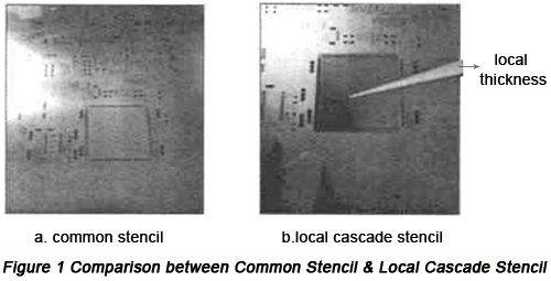
In the early stage of stencil design, the thickness of stencil is designed t be 0.13mm because of QFP components with pin distance of 0.5mm on PCB. In the first manufacturing process, false welding takes place to core module with the thickness of tin paste to be 0.13mm, based on which the thickness of stencil is increased to the minimum thickness of common stencil design that is 0.15mm. Under this condition, the proportion of stencil hole and outside enlarge hole is 1:1.2 with the bad quality far from being improved. Under this condition, only special cascade stencil can be applied in the experiment and the thickness of stencil is improved to 0.3mm from the original 0.15mm so that the tin paste printing amount in the module mounting pad can be ensured.

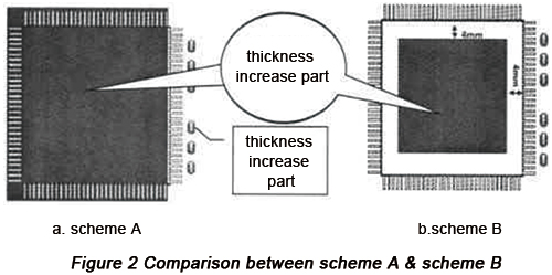
Different experiment schemes are used during cascade stencil application and relatively reasonable schemes are displayed in the following:
In Scheme A, the thickness of overall area of the module is increased by 0.3mm with the thickness of the side containing small scale unchanged.
In Scheme B, the area with thickness to be increased is 4mm smaller than that in Scheme A and the thickness is increased by 0.3mm with the thickness of pad holes unchanged.
After the pilot production and comparison between Scheme A and B, continuous tin electrodeposit takes place at the resister pack position, based on which it can be concluded that Scheme B is better.

c. Manufacturing craft improvement experiment
Prior to reflow oven entry, the task of gel dispensing has to be implemented and positions can be determined under the effect of gel solidification and shrinking with the function of circuit module fixing so that deformation and displacement of module substrate can be effectively reduced when soldering.
• Experiment result
Thanks to a series of improvement measures including stencil design improvement, reselection and positioning of PCB material and improvement of manufacturing craft, the amount of tin paste and climbing height of tin in the core module have reached IPC Standard in the process of soldering. The fraction defective of core module process is greatly reduced from 686PPM to 23PPM so that the reliability of products is ensured.
The data in the following table best indicates the result.
|
Result
|
Substrate material
|
Production Volume
|
Number of
Test points
|
Defect type
|
Number of Defect
|
Number of Badness
|
Fraction defective (PPM)
|
|
Initial Pilot Production Circumstance
|
Tg150
|
50
|
43750
|
False welding of core module
|
20
|
20
|
457
|
|
Continuoustin electrodeposit
of core module
|
0
|
0
|
0
|
|
Sum
|
20
|
20
|
457
|
|
Experiment Result for the First Time of Improvement (scheme A)
|
Tg170
|
50
|
43750
|
False welding of resistor pack
|
0
|
0
|
0
|
|
Continuous tin electrodeposit
of resistor pack |
30
|
30
|
686
|
|
Sum
|
30
|
30
|
686
|
|
Experiment Result for the Second Time of Improvement (scheme B)
|
Tg170
|
50
|
43750
|
False welding of core module
|
1
|
1
|
23
|
|
Continuous tin electrodeposit
of core module |
0
|
0
|
0
|
|
Sum
|
1
|
1
|
23
|
The application of core module is capable of accelerating the research development and upgrading progress of automotive electronic products. In the stage of new products, transplantation can be implemented so that development cost and complexity can be reduced. However, bad points come up in the early stage of pilot production as a result of the large scale of core module and high manufacturing craft requirement so that its reliability will possibly shrink and the module fails to be better applied.
Belonging to PCB, core module has to go through a series of processes including high temperature reflow, storage and another high temperature reflow during which PCB deformation, false welding and continuous tin electrodeposit. These problems concerning core module have been successfully solved through experiment and pilot production of products so that more opportunities will be provided for the application of core modules and the module application progress of automotive electronic products will be accelerated as well.
Helpful Resources:
• Elements Influencing SMT Soldering Quality and Improvement Measures
• Automotive PCB Properties and Design Considerations
• 5 Tips for Automotive Circuit Design to Defeat EMI
• 5 Proven Ways to Judge Reliability of Automotive PCB Manufacturers
• Some Handy Methods in Evaluating SMT Assembler's Capabilities
• Full Feature PCB Manufacturing Service from PCBCart - Multiple Value-added options
• Advanced PCB Assembly Service from PCBCart - Start from 1 piece


