As a platform for components whose applications can be well implemented in electronic products, PCBs (Printed Circuit Boards) play a key role as electric connection between components and account for the base in electronic devices or equipment. Therefore, its performance and quality directly leads to that of electronic products. Along with rapid development in microelectronics technology, numerous electronic products tend to work together so that interference between them increasingly climbs up. Furthermore, increasing PCB density leads to the fact that the quality of PCB design plays a critical role in determining the extent of interference and interference resistance. As a result, apart from component selection and circuit design, excellent component layout and routing also contribute to PCB EMC (ElectroMagnetic Compatibility) design if circuit is required to capture optimal performance.
EMC refers to device or system capability that they are capable of normally working in electromagnetic environment while refusing to generate unacceptable electromagnetic interference to ambient devices or systems. Electromagnetic interference is formed due to multiple reasons primarily summarized into extraordinarily high working frequency or unacceptable layout or routing. Under the background of unavoidable high radio frequency (RF), designers should focus on component layout, routing, power and grounding design when implementing PCB design for concern of EMC. Moreover, for PCBs with different count of layers, different design elements should be taken into consideration to achieve optimal performance.
Interference Source
• Differential-mode Current and Common-mode Current
a. Differential-mode transmission and Common-mode transmission
Any circuit contains common-mode (CM) current and differential-mode (DM) current. Both of them decide the extent of RF transmission. As a matter of fact, huge extinction exists between them. When a couple of leads or traces and a reference return source are given, either type of current will be available. Generally speaking, DM signals carry data or useful information. Common mode, however, causes most trouble to EMC as negative effect of DM current. DM transmission is usually defined as transmission from line to line while CM transmission is usually defined as transmission from line to ground. The maximum field intensity generated by closed loop can be figured out by formula  . E refers to the max field intensity (μV/m); r refers to the distance between closed loop and measuring antenna (m); f refers to frequency (MHz); Is refers to current (mA); A refers to the area of loop (cm²).
Based on the formula above, it is clearly indicated that field intensity is directly proportional to the loop area. To reduce DM transmission level (TL), loop area should be shrinked apart from source current reduction.
CM radiation results from voltage drop causes partial grounding voltage to be higher than that in reference ground. Cable connected with influential grounding system is regarded as antenna that is a component of CM radiation. Far-field component can be depicted by formula 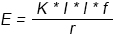 , K refers to transmission coefficient; I refers to CM current (A); l refers to cable length (m); f refers to transmission frequency (MHz); r refers to distance (m).
This formula clearly indicates that field intensity is directly proportional to cable length. CM transmission reduction depends on CM current decrease and cable length lowering.
b. Conversion between CM and DM
DM and CM can be mutually converted when two signal lines with different impedance are available. The impedance is mainly determined by leads or comb-shaped capacitor and inductor that are correlated with physical tracing. For tracing of majority PCBs, parasitic capacitance and inductance should be well controlled to minimum so that CM and DM can be avoided being generated. Therefore, circuits that are sensitive to the environment have to reach balance through a certain method so that leads or comb-shaped capacitance of each conductor are equivalent to parasitic capacitance.
c. General method of stopping CM and DM interference
The fundamental guideline to stop CM and DM current and RF interference lies in current capacity offset or current capacity minimization. As current flows in traces, magnetic lines of force are generated, leading to the occurrence of electric field. Both fields are capable of radiating RF energy. If magnetic lines of force are offset or decreased to minimum, RF energy won't exist anymore, which will finally stop interference. Specific measures or rules that can be conformed to will be discussed in the latter part of this article.
• Crosstalk
As a crucial element of PCB design, crosstalk has to be carefully considered in each link of the whole process. Crosstalk refers to unwanted electromagnetic coupling between traces, leads, cable bunches, components or other electronic components that tend to be influenced by electromagnetic interference.
As a leading EMI (ElectroMagnetic Interference) transmission approach, crosstalk tends to cause interference between traces. Crosstalk can be classified into capacitance coupling and inductance coupling. The former usually derives from the fact that trace is located over other traces or reference plane. The latter usually derives from traces that are physically approximate to each other. When it comes to parallel traces, crosstalk features two modes: forward and backward. For PCBs, backward crosstalk is more worth considering than forward crosstalk. In circuits, the larger impedance is between power and interfered traces, the higher crosstalk level will be. Inductance crosstalk can be controlled by adding edge-to-edge distance between traces and transmission lines or leads or minimizing distance between traces and reference plane.
• Digital Signal Spectrum Analysis
a. Digital signals
Attribute of digital signals is square wave and square wave signals are composed by fundamental wave and lots of harmonic sines. Fourier transform can be applied to capture digital signals' frequency range waveform. Therefore, the shorter pulse repetition period is, the higher its repetition frequency will be and so will harmonic frequency be. Theoretically, rising time of square wave is zero so that harmonic content is infinite. However, it's a trapezoidal waveform with both rising edge and falling edge.
b. Pulse time domain and frequency domain conversion (Fourier transform)
Fourier transform leads rectangular pulse to be discomposed into cosine or sine waves, conforming to formula 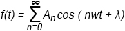 . In this equation, ADn refers to the amplitude of each cosine waveform; n refers to the count of harmonic waves; w refers to angular frequency.
• Decoupling and Grounding
a. Decoupling design
Composed by inductor and capacitor, low-pass filter is capable of filtering high-frequency interference signals. Parasitic inductance on lines will slow down power supply so that output current of driving devices will go down. Appropriate placement of decoupling capacitor and application of energy storage function of inductor and capacitor make it possible to supply current to devices at the moment of on and off. In a DC loop, load change will arouse power noise. Decoupling capacitor configuration can stop noise from being generated due to load change.
b. Grounding design
For electronic devices, grounding is a crucial method to control interference. If grounding is correctly combined with shielding measures, most interference issues will be solved.
• Component layout and routing
Circuit layout directly determines the extent of electromagnetic interference and intensity of interference resistance. Appropriate layout not only increases circuit efficiency, but improves EMC of the whole system as well. The higher working frequency of unit circuit becomes, the higher speed will be and the more diversifying signal spectrum will be. Consequently, the higher proportion of high-frequency component is, the stronger interference will be. From the perspective of frequency, first comes high-frequency circuit, then mid-frequency circuit and finally low-frequency circuit. From the perspective of logic speed, however, first comes high-speed circuit, then mid-speed circuit and finally low-speed circuit. In accordance with that theory, circuit layout should be implemented conforming to the following design.

Apart from classification according to frequency or speed, function and type can also be used as classification standard. Detailed measures to be taken will be discussed in the rest part of this article soon. Keep on reading and you'll obtain them in detail.
PCB Design Rules for EMC
Since interference sources calling for damage to EMC performance of circuits have been dug out, corresponding design rules for EMC concern should be worked out catering to those sources. Here are PCB design rules to achieve EMC success.
• Surface Layout
a. PCB size has to be considered. When it comes to boards with extraordinarily large size, tracing has to go a long way with impedance increased, noise resistance reduced and manufacturing cost rising. When it comes to boards with extraordinarily small size, trouble will be caused for thermal dissipation and crosstalk tends to take place between adjacent traces. Recommended PCB size is rectangular shape with ratio between length and width to be 3:2 or 4:3. Furthermore, when board size goes beyond 200mm*150mm, mechanical intensity withdrawn by board should be considered. Thus, it is very important that you know your PCB manufacturer's limit on board dimension. For instance, PCBCart can print circuit boards in min 6*6mm and max 600*700mm. Check its custom PCB manufacturing capabilities for more details.
b. Partitioning should be carefully considered for component layout design. Digital circuits, analog circuits and noise source should be independently placed on board and high-frequency circuit should be isolated from low-frequency circuit. Moreover, attention should be paid to component distribution with strong and weak signals and signal transmission direction issue.
c. Layout should center on core component in each function circuit to ensure component be trimly and compactly positioned along the same direction. To stop coupling between signals from being formed, components easily influenced by interference shouldn't be neighborly positioned.
d. Sensitive-signal components should be far from power and high-power devices and sensitive-signal lines are never allowed to go across high-power devices. Thermally-sensitive components should be positioned far from thermal devices while temperature-sensitive components should be positioned at the area with the lowest temperature.
e. Distance should be enlarged between components with a high potential difference in order to avoid the possibility of occurrence of short circuit. Plus, high-power components should try to be arranged at places that are inaccessible to hand touch in testing and go through insulation protection.
f. A through hole will bring distributed capacitance of 0.5pF, so a reduction of through holes is beneficial to operating speed improvement.
• Component Layout
a. Compared with discrete components, IC components should receive priority selection owing to their advantages of excellent packaging, fewer solder joints and low rate of failure. Moreover, devices with a relatively slow signal slope should be selected so that high-frequency sections generated by signals can be reduced. Application of surface mount devices can reduce tracing length with impedance reduced and EMC improved.
b. Components should be positioned based on the same classification. Incompatible components should be independently placed to ensure that components won't interfere with each other in space.
c. Components weighing over 15g shouldn't go through soldering until they have been fixed by support. Components that are both large and heavy and generate much heat shouldn't be assembled on board; instead, they should be assembled on the bottom board of finished box. Furthermore, thermal dissipation has to be guaranteed and thermally-sensitive components should be far from components generating heat.
d. When it comes to adjustable components such as potentiometer, adjustable inductance coil, variable capacitor and micro switch, structural requirement of the whole system should be considered. Those components should be placed on circuit board if inner adjustment is called for while they should be at places compatible with machine board if outer adjustment is required.
• Routing design
General routing rule conforms to the following sequence:

Apart from that general routing rule, some details should never be ignored:
a. To minimize radiation interference, multi-layer PCBs should be picked up with inner layers defined to be power plane and ground plane so that power circuit impedance can be reduced and public impedance noise can be stopped with even grounding plane to be generated for signal lines. It plays a key role in stopping radiation by improving distributed capacitance between signal lines and grounding plane. More design notes for multi-layer PCBs are depicted in the section of PCB Layer and EMC Design below.
b. Low impedance should be maintained on high-frequency signals by power lines, grounding lines and traces on circuit board. When frequency is kept so high, power lines, grounding lines and circuit board traces all become small antennas responsible for receiving and transmitting interference. To defeat such interference, compared with adding filtering capacitors, it's more important to reduce high-frequency impedance owned by power lines, grounding lines and circuit board traces. Therefore, traces on circuit board should be short and thick and evenly arranged.
c. Power lines, grounding lines and printed traces should be appropriately arranged so that they can be short and straight to minimize loop area formed by signal lines and return lines.
d. Clock generator should be as close to clock devices as possible.
e. Shell of quartz-crystal oscillator should be connected with ground.
f. Clock domain should be encircled by grounding lines and clock lines should be as short as possible.
g. Broken lines with an angle of 45° instead of 90° should be applied for circuit board to decrease transmission and coupling of high-frequency signals.
h. Single-point connection with power and single-point connection with ground should be applied on single-layer PCB and double-layer PCB. Both power lines and grounding lines should be as thick as possible.
i. I/O driving circuit should be close to connectors at the edge of circuit board.
j. Key lines should try to be thick and protection ground should be added to both sides. High-speed lines should be short and straight.
k. Component pins should be as short as possible, which works especially for decoupling capacitors utilize mounting capacitors with no pins.
l. When it comes to A/D components, grounding lines in digital section and analog section mustn't be crossed.
m. Clock, bus and chip select signals should be far from I/O lines and connectors.
n. Analog voltage input lines, reference voltage terminal should be far from digital circuit signal lines, especially clock.
o. Interference is smaller when clock lines are vertical to I/O lines than parallel to I/O lines. Moreover, clock component pins should be far from I/O cables.
p. Tracing should never be arranged under quartz crystal or devices sensitive to noise.
q. Current loop should never be generated around weak-signal circuits or low-frequency circuits.
r. Any signal shouldn't make loop generated. If a loop has to be arranged, it should be as small as possible.
• Trace routing
a. Parallel layout should be carried out on current signals with the same output but opposite directions to eliminate magnetic interference.
b. Discontinuity of printed leads should be reduced at utmost. e.g. lead width shouldn't go through a sudden change with leads' corner to be over 90°.
c. EMI tends to be generated by clock signal lines most and clock signal lines should be close to grounding loop in the process of routing.
d. Bus driver should be next to the bus to be driven. When it comes to the wires away from PCBs, drivers should be placed next to connectors.
e. Since signal lines of clock leads, row driver or bus drivers usually carry large transient current, printed leads should be as short as possible. For discrete components, printed lead width can reach approximately 1.5mm. For ICs, however, width of printed leads should between 0.2mm to 1.0mm.
f. Large-area copper foil should be avoided being used around thermal devices or leads with large current flowing through, otherwise issues such as copper foil inflation or falling will possibly be caused if products remain in thermal environment for a long time. If large-area copper foil has to be used, it's better to take advantage of grid, which is beneficial to eliminate escaping gas generated due to thermal adhesion between copper foil and substrate.
g. Via aperture at the center of pad should be suitably larger than that of component pins. Dry soldering tends to be generated if pads are too large.
• Power design
Inappropriate power design leads to large noise generation, which eventually reduces products' performance. Two primary factors cause unstable power:
#1: In the state of high-speed switching, transient exchange current is too large;
#2: Inductance exists on current return.
As a result, integrity of power should be fully considered in PCB design, apart from which the following rules should be stuck to as well.
a. Power decoupling filtering design
Bridging of a decoupling capacitor with capacitance from 0.01μF to 0.1μF at two terminals of IC chip power can dramatically reduce noise and surge current across the board. With current compensation fulfilled, the lower decoupling capacitance, the better. Mounting capacitors should be optimally used due to its low lead inductance.
The most effective method to filter power lies in filter arrangement at AC power supply wire. To stop leads from mutually coupling or loop from occurring, input and output lines of filter should be directed from both sides of circuit board and leads should be as short as possible.
b. Power protection design
Power protection design covers over-current protection, lack-voltage alarm, soft start and over-voltage protection. Over-current protection can be achieved in power section of PCB through the application of fuse. To prohibit fuse from affecting other modules in the process of melting, input voltage should be designed as well to maintain capacitance. To stop over voltage from damaging components by accident, an equal potential should be established through protection devices such as discharge tube and varistor between distribution line and ground potential to accomplish over-voltage protection.
• Ground design
For device of equivalent potential with electric potential base point, ground wires features inconstant potential. Relatively large distinctions may be observed when use meter to measure potential between points on ground wires, which will eventually cause errors when circuit is working.
The leading reason for EMI by ground wires lies in impedance on ground wires. When current is flowing through ground wires, voltage will be generated, which is actually ground noise. Under the driving of such voltage, loop current on ground wires will be caused, which thereafter generates ground loop interference. If two circuits commonly use the same ground wire, public impedance coupling will take place.
Solutions for ground loop interference contain ground loop cutting, ground loop impedance adding and application of balanced circuit. Methods to defeat public impedance coupling lie in impedance reduction on public ground wire or parallel single-point grounding. Specific rules in terms of ground wire design goes like the following.
a. Separation between digital ground and analog ground
If both analog circuits and linear circuits are available on circuit board, they should be isolated from each other. Low-frequency circuits should depend more on single-point parallel grounding. When troubles occur in practical routing process, series grounding can be partially implemented before parallel grounding. High-frequency circuits tend to depend on multi-point series grounding and grounding wires should be short and thick. Grid-shaped copper foil should be massively applied around high-frequency components.
b. Ground wires should be as thick as possible
Grounding wires should be as thick as possible so that current twice larger than allowable current of PCB can go through to increase noise resistance. If copper pouring is applied to make ground wires, dead copper should be avoided. Moreover, copper with similar functions should be connected with each other through thick leads so that quality of ground wires can be ensured with noise reduced.
c. Closed-loop circuit formed by ground wires
For circuit board containing only digital circuits, noise resistance capability can be increased by designing grounding circuit into circular loop.
PCB Layer and EMC Design
• Appropriate PCB Layer Count
In terms of layer count, single-layer PCBs, double-layer PCBs and multi-layer PCBs.
a. Single-layer PCBs and double-layer PCBs are applicable for mid/low-density routing or low-integrity circuits. Based on manufacturing cost concern, most consumer electronics products depend on single-layer PCBs or double-layer PCBs. Nevertheless, both of them generate much EMI as a result of defects of their structures and they are sensitive to external interference as well.
b. Multi-layer PCBs tend to be more applied in high-density routing and high-integrity chip circuits. Therefore, when signal frequency is high with electronic components distributed in high density, at least 4-layer PCBs should be selected. In multi-layer PCB design, power plane and ground plane should be specifically arranged with distance between signal lines and ground lines reduced. As a result, loop area of all signals can be magnificently decreased. From the perspective of EMC, multi-layer PCBs are capable of effectively reducing radiation and improving anti-interference capability.
• Single-Layer PCB Design
Single-layer PCBs usually work at a low frequency of several hundred KHz as lots of design conditions of high frequency are limited due to low-frequency limits such as lack of RF circuit return and control conditions required by complete closure, obvious line skin effect or unavoidable magnetic and loop antenna issues. Therefore, single-layer PCBs tend to be sensitive to RF interference like static electricity, fast pulse, radiation or conducted RF. In single-layer PCB design, signal integrity and terminal matching are taken into no consideration. First comes power and ground wire design, then high-risk signal design that should be placed next to ground wire. The closer, the better. Finally comes the design of other lines. Specific design measures include:
a. Power and ground wires must be ensured to go along power box grounding points in key circuit signal network.
b. Traces should be routed according to sub-functions and design requirement has to be critically considered on sensitive components and corresponding I/O terminals and connectors.
c. All the components in critical signal network should be adjacently placed.
d. When PCBs call for multiple grounding points, make sure those points be mutually connected with each other and include connection method design.
e. For other lines routing, lines with higher capacity of RF withstanding should utilize design method of mini pass with RF return path clear through the way.
• Double/Multi-Layer PCB Design
a. Key power plane should be arranged adjacent to corresponding ground plane with coupling capacitance generated. Cooperating with PCB decoupling capacitor, key power plane is beneficial to impedance reduction on power plane with excellent filtering effect acquired.
b. Key signals on adjacent planes aren't allowed to go across splitting zone to stop signal loop enlarging, to decrease intense radiation and reduce interference sensitivity.
c. Key signals such as clock signals, high-frequency signals and high-speed signals call for an adjacent ground plane. For example, signal plane adjacent to ground plane can be regarded as an optimal plane for signal routing so that signal loop area and shielding radiation can be shrinked.
d. Power plane should be smaller than ground plane usually due to conformation to 20H rule.
EMC design for PCBs derives from complexity of techniques, knowledge and experience. All the design rules listed in this article aim to provide fundamental and conceptual guidelines for engineers to ensure their first success in EMC design. As a matter of fact, excellent EMC design demands engineers to take as many elements as possible into board design account and engineers should know what they are and how to react to them.
Helpful Resources:
• The Most Comprehensive Introduction of EMI and EMC Automated Tools
• PCB Layout Influence of Electronic Product EMC Performance
• PCB Partitioning Design Rules for EMC Improvement
• PCB Design for Radio Frequency Circuit and Electromagnetic Compatibility
• Three Design Considerations Ensuring EMC of Laptop PCB
• Full Feature PCB Manufacturing Service from PCBCart - Multiple Value-added options
• Advanced PCB Assembly Service from PCBCart - Start from 1 piece


