Switching power supply technology has witnessed a development towards miniature, high frequency and high efficiency with the development of highly integrated chips in recent years. Highly integrated control chips make required peripheral components become simplified since it's relatively easy to design a switch power supply depending on the design software. However, the problem of high integration leads to low freedom of design, low availability of chips and low price. Design software developed by each manufacturer is just capable of simulating some types of peculiar chips. In the practical application, it is crucial to design a switch power supply compatible with product demands with excellent running conditions. Based on the requirement of power module for RFID, a switch power is designed with a voltage from 220VAC to 0.5VDC and a dimension of 88mm x 70mm. Since the running current is close to 1.5A in the process of reading tags, the maximum output current of designed switch power is set to be 3A.
In the design of miniature with relatively low output power, according to Erickson R W theory, the power switch availability of flyback switch power that is 0.385 is more than 0.353 that uses the type of normal shock, full bridge and half bridge. Therefore, flyback converter structure is picked up. Taking the advantages of feedback design and current mode controller into consideration, current mode PWM control chip UC3842 is picked up.
In the switch power applying the chip UC3842, peripheral circuit design is relatively easy. Current mode PWM control chip structure eliminates the double pole brought by inductance in the loop in order to effectively simplify the design of feedback loop. Output terminal feedback style is applied consisting of stabilovolt tube TL431 and optocoupler. In the design based on UC3842, designers tend to independently design each module in the flyback structure, emphasizing design of adjacent circuit and feedback circuit, with other circuit design neglected. For example, according to extra element theorem by Dr. Middlebrook, input impedance of input filter has to be far smaller than input impedance of converter. Otherwise, fluctuation possibly takes place to circuit. This design carefully discusses adjacent circuit design such as circuit design of input filter, slope compensation and ground circuit design. Design scheme is determined through Saber simulation and its compatibility with requirement and stability through debugging with RFID.
Basic Theory of Flyback Switch Power
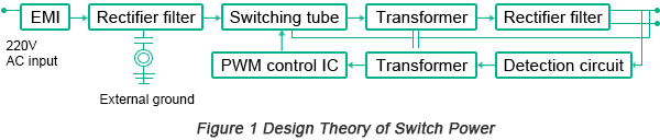
The basic design theory of switch power is to transform VAC into VDC for the power supply to IC chip changing DC to HFAC which then changes into DC output. Feedback stabilizes output voltage from output DC sample and input IC control switch. The theory of switch power is illustrated in Figure 1.
Current mode double closed-loop structure is applied in control converter of flyback switch power. The feature of flyback converter lies in the fact that in the closed condition of switching tube, the inductance energy inside the coils on one side of transformer provides power for the carrier through rectifier diode while in the open condition of switching tube, energy is stored inside the coil of transformer and the output is provided by energy stored inside output capacitor. The schematic diagram of flyback converter is illustrated in Figure 2.
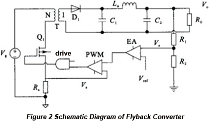
When the voltage detected by output detection resistors R1 and R2 is less than reference voltage Vref, error rises through error amplifier with switching tube Q1 open. The primary inductance and current of transformer rise by the slope of (Vg - Von)/ Lm. Sampling resistor Rs changes primary inductance and current into sampling voltage. Based on the comparison between the sampling voltage on sampling resistor Rs and error voltage, when the voltage on sampling resistor Rs rises to the value that is higher than error voltage, low level will be output and switching tube is closed until the coming of next clock. Flyback switching power doesn't need output power inductor and inductor of transformer can be directly applied for power that features a simple topological structure. Control circuit mainly depends on current mode PWM chip UC3842 and peripheral circuit.
Current Mode PWM Chip UC3842
The control CPU applied in this design is PWM chip UC3842 in the mode of fixed frequency and current, integrating crucial control components such as oscillator, error amplifier, PWM comparator and SR trigger. This chip features the functionality of under-voltage and over-current protection with an output mode of totem pole, working frequency of 500kHz, starting current less than 1mA and the maximum output current of 1A.
The functions of pins are different from each other. Pin 7 is for power supply. When voltage is more than slow start threshold of 16V, Schmitt trigger outputs high level. Voltage regulator supplies reference voltage of 5V to pin 8 and when the voltage is lower than 10V, Schmitt trigger outputs low level with undervoltage locked. Internal stabilivolt tube limits the maximum input voltage within 36V. Power is supplied to Ct by pin 4 through external RC circuit and by pin 8 through resistor Rt and Ct determines the frequency of oscillator through internal current source generating electricity. Pin 2 is the inverting input of error amplifier while pin 1 is the output of error amplifier to supply compensation. Pin 3 is the pin of current detection, determining the duty cycle through the output of error amplifier and when the voltage of pin 3 is more than 1V, current flow is closed. Pin 6 supplies totem pole mode output with the maximum working current of 1A, accelerating the closing of switching tube.
Design of Flyback Switch Power Control
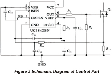
The schematic diagram of control part is displayed in Figure 3 below. The control part of flyback converter is mostly integrated inside the chip UC3842 and only a few external components can implement the required control function. The main control function module includes starting circuit, frequency design, protection circuit, driving circuit and slope compensation.
• Starting circuit and frequency design
Starting circuit supplies pin 7 starting voltage of more than 16V. When the system starts, power is supplied to pin 7 by auxiliary winding. The working frequency of this system is determined by timing capacitor and resistor between pin 8 and pin 4. The 5V reference voltage of pin 8 provides power to capacitor C15 through resistor R9. Capacitor C15 then generates sawtooth wave through internal current source generating electricity whose time span determines the dead time of chip outputting PWM. In order to ensure the performance, dead time should be less than oscillation period by 5%. Based on timing sequence diagram, it can be obtained that C15 is 3.3nF and working frequency 47kHz. In accordance with the formula fosc = 1.7/( Rref x C15), the value of R9 is 11kHz.
• Current foldback circuit
The current foldback circuit of chip transforms inductor current at the primary edge into the output voltage of voltage and error amplifier implemented by PWM comparator through over current detection resistor. When the voltage of pin 3 is more than 1V, output breaks down. Peak inductor current is supposed to be 1A and the value of current detection resistor R13 is supposed to be 1Ω. In order to prevent the error shutoff led by inductor current peak of transformer primary edge, R11 and C14 are accessed to filter peak and the peak current is approximately hundreds of nanoseconds. In the condition that R11 is supposed to be 1k and C14 500pF, time constant τ = RC = 500ns.
• Driving circuit of MOS tube
The driving circuit of MOS tube is responsible for the excellent wave form of PWM, especially the fall edge. The serial connection between output pin 6 and grid series resistor R6 will decrease the high-frequency parasitic fluctuation caused by MOS tube input capacitance and any serial lead inductance in the circuit. In order to ensure MOS tube switch PWM waveform, the value of R6 is always small in the range from tens to twenties ohm. The value of R8 is supposed to be 15kΩ as MOS tube grid bleeder resistor.
• Slope compensation
In the peak current mode control, the peak value of inductor current is constantly set while the average value of inductor current isn't. The change of duty cycle will change the average current and the inner ring of peak current control ensures the peak value of inductor current but fails to control the correct inductor current average value compatible with output voltage, leading to the constant change of output voltage. When the duty cycle is more than 50%, the inductor current fluctuation will generate oscillation. In this design, slope compensation is required. The application of upper slope compensation refers to a stack of positive slope voltage on current sample signals. Capacitive compensation is applied in this design with a C51 of 100pF added between pin 3 and pin 4 and the oscillation signal of oscillator supplies power to C51 and pin 3 through capacitor. With this type of slope compensation, capacitance is relatively small with a rank of pF to avoid attracting the current of oscillator and generating too large negative voltage on pin 3.
Peripheral Circuit Design of Flyback Switch Power
• Circuit design for EMI and rectifier filter
In order to filter the interference of high-frequency power grid to devices and the influence of high-frequency switch to power grid, EMI filter circuit should be accessed by input rank. The circuit diagram of common EMI filter wave is shown in Figure 4.
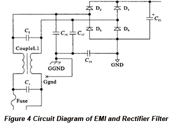
C1 is connected at the input port of power grid while C2 is with input port of device to eliminate differential mode interference. L shares the same direction with common mode choke to filter common mode interference while C16 and C17 are connected with ground to filter common mode interference.
The leak current of C16 and C17 is calculated conform to formula:  . For two identical capacitors, the amplitude of leak current should conform to formula:
  , in which f refers to the frequency of power grid with the value of 50Hz, C refers to the overall capacitance of 4400pF to the ground, and V refers to the ground voltage of 110V. Therefore, the value of Ileak is 0.15mA that is compatible with the alternating current with the valid value of 220VAC after EMI compatible with security standard. The amplitude is
  while the output DCV is
  . The reverse breakdown voltage of diode should meet the following requirement:
  . C refers to filter capacitance while RL refers to load. The larger the time constant RLC is and the smoother capacitance is, the better the filter effect will be. The diode ln4007 with a high withstand voltage is picked up.
• Oscillation brought by filter output impedance and converter input impedance
The incompatibility between the input impedance of converter and output impedance of filter possibly leads to oscillation as well. The input impedance of converter of loop system can be regarded as a negative resistor (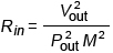 ). Filter is LC filter and the transfer function can be obtained with ESR of inductance and capacitance.
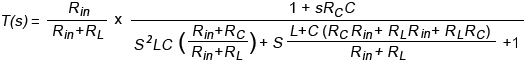
The input impedance of converter of system constant oscillation should conform to the formula: 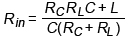 .
.
Therefore, only if the input impedance of loop converter is less than calculated filter oscillation output impedance, the damping coefficient of transfer function is positive value that will become steady in order to reduce oscillation. Otherwise, the circuit will fluctuate.
• Snubber circuit design
In order to prevent the frequency tube from being destroyed as a result of shutoff overvoltage, primary edge RCD snubber circuit has to be assembled to transformer. The output port break down the output diode to prevent hard breakdown with output snubber circuit added, which is illustrated in Figure 5.
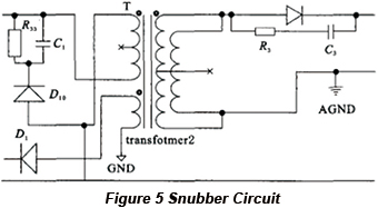
In the process of breakdown of MOS tube, the current of primary edge id supplies power to the parasitic leakage source capacitance through transformer primary edge leakage source. This high-frequency voltage may make the voltage on the switch tube exceed withstand voltage and break down switch tube so an RCD snubber circuit is added to provide a voltage tapping path. Fast recovery diode FR107 with high withstand voltage is picked up, RCD resistor 5kΩ and capacitance 3300pF.
When input is open with MOS tube opened, the voltage added on output schottky diode (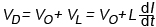 ) and the hard breakdown of MOS tube leads to the breakdown of diode. With RC snubber circuit added, the voltage on schottky diode VD = VO + IO x R3. The open time of 2SK792 of MOS tube is 55ns, the reverse withstand voltage of schottky diode SB540 is 60V, output VO is 5V and the max current is 3A. Therefore, the equivalent resistance of the max snubber circuit is 18.33Ω and (
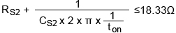 ). When R is 18Ω and C is 560pF, the equivalent serial resistance is 18.06Ω.
• Output circuit design
Rectification is implemented by output part through schottky diode and filtering applies capacitor with low ESR with equivalent capacitor ESR reducing output, which is shown in Figure 6.
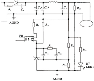
Output sampling circuits are obtained through R5 and R12 differential voltage and the value of R12 is determined with reference of TL431 output terminal current that is 1.5μA. In order to avoid the current influencing differential voltage ratio and noise, the current through resistor R12 should be more than 100 times of TL431 input current. Rlow<2.5/150μA=16.6kΩ. Since the working current of TL431 is in the range from 1mA to 100mA, when the current of R5 is nearly 0, the current of 1mA is provided to TL431 by R14 (R14<Uf /1mA). Based on the manual of PC817B, Uf = 1.15V, the value of R14 can be 1kΩ since its value should be less than 1.15 kΩ.
Based on the feature curves of triode in PC817B, when the forward current of transistor is approximately 7mA, the value of IC is 7mA as well and the emitter voltage is linear within a relatively wide category with uc3842comp linear. The CTR in PC817B is in the range from 1.3 to 2.6. When the value of IC is 7mA, with the worst situation considered, the value of CTR is 1.3. The maximum current flowing through LED is required to be If = IC/1.3 = 5.38mA, R4<(5 - Uka - Uf)/5.38mA = (5 - 1.15 - 2.5)/5.38mA = 250Ω. The maximum current TL431 can withstand is 150mA while the maximum current PC817 can withstand is 50mA. Therefore, the maximum current R4 provides is 50mA with R4>(5 - 1.15 - 2.5)/50mA = 27Ω. So the range of R4 is between 27Ω and 250Ω with the value of 150Ω selected.
• Ground circuit design
Transformer is applied for ground isolator between cold and hot ground in switch power. The hot ground at the primary edge of transformer can be formed into loop through electric grid and the secondary transformer refers to the loop formed by cold ground and ground. Safety capacitor Y is picked up by C16 and C17 to connect zero line and firing line to frame ground to filter common mode interference. Capacitor C18 between hot ground and cold ground transforms noise at the secondary side of transformer into the primary short circuit to reduce radiation electromagnetic wave.
Helpful Resources
• A Comprehensive Introduction of IoT Based on RFID
• Design of High-Power PCB in High Temperature Environment
• How to Defeat Control Power Supply Grounding Defects Based on Insulation Reduction in PCB Design
• Discussion on Power and Ground in Electromagnetic Compatibility of PCB
• How to Analyze and Prohibit Impedance of High-Speed PCB Power
• Aluminum Backed PCBs: The Solution to High Power and Tight Tolerance Applications
• Full Feature PCB Manufacturing Service from PCBCart - Multiple Value-added options
• Advanced PCB Assembly Service from PCBCart - Start from 1 piece


