Modern electronic system is developing in the trend of small package, large scale and high speed as the density of chips is becoming increasingly large in SLSI (super-large-scale integration), which brings about some inevitable problems such as how to analyze and deal with the interconnections and stacking problems in high-speed circuit design. At present, the radio frequency of electronic products reaches hundreds or thousands of MHz and both the rising edge and falling edge become so steep that PCB layout rules and dielectric constant of substrate material are extremely crucial to the electric performance of the system in the process designing such products.
As a significant process and step in the majority of present electronic product research, high-speed PCB design has seen the main issues including timing problem, noise interference and EMI (electromagnetic interference) whose solutions are related with the normal operation of system design.
Now, traditional design methods lead to the low reliability and success rate of products, which provide high practical value and wide market expectations for research on high-speed PCB design in embedded application system.
Figure 1 shows the function frame of embedded RTU (remote terminal unit).

From Figure 1, it can be seen that this system is a vertical communication structure composed by data accumulation layer containing electricity energy unit, sensor unit and analog amount measurement unit, data transmission layer containing gateway that adjusts the data in the data accumulation layer through the command from Internet receiving engineer center and data processing layer that is implemented by APP monitoring software, store and analyze data at real time and to make data curves faced to user interface so that the flexibility and administration efficiency of data accumulation are increased.
This embedded IoT RTU system hardware mainly consists of USB2.0, AT91SAM9263 processor, CAN, SDRAM, Nand Flash, Data Flash, Ethernet controller, clock chip, RS232/485 interface, power administration and data accumulation parts.
Operated by Linux operation system, this design features higher capabilities of memory and device administration so that multi-mission real-time scheduling is implemented containing complex algorithm and communication protocol to be responsible for network connection, data communication and configuration accumulation. Figure 2 is the RTU circuit board designed in this article.

Supporting the dual stack of IPv6 and IPv4, this system is capable of implementing the promptness and real-time capability. In terms of data storage, the requirement of local storage can be met under the condition of communication block. In terms of communication interface, it features different field data communication interfaces including RS485, RS232 and CAN, supporting Modbus RTU communication protocol and meeting requirement of different interfaces and different communication rates.
• PCB stacking up design of the system
The number of layers of PCBs is usually in the range 2 to 32 based on the difficulty of design. The 6-layer PCB in this design is determined according to component package density, small layout routing space and high signal frequency. This PCB layer distribution is illustrated in Figure 3 below.

Strip lines configuration is picked up for FLASH and SDRAM in this system and routing is implemented on Inner Signal 1 and Inner Signal 2.
• PCB constraint rules in this system
During high-speed PCB design, impedance continuity and EMI are greatly influenced by spacing, length and width of wires and adjacent processing of loops. The quality of component layout and routing is related with the success of the final design so PCB constraint rules have to be reasonably enacted.
Hyper Lynx features a functionality of interfering with chart analysis and IBIS model can be applied to accurately simulate loss transmission, differential signals and through-hole model that changes with frequency. The main network is simulated before routing by Line to improve PCB stacking structure and routing impedance and high-speed PCB network routing constraint rules are designed before simulation result to increase design efficiency.
• PCB simulation of this system
In the process of high-speed PCB design, an ideal transmission line model is applied for front terminal simulation with limited signal lines simulated for one time. The transmission lines at PCB back terminal, however, are actually routing lines of PCB with influence of through-hole and planes shift. Under this circumstance, the obtained simulation result is extremely reliable.
In the process of core circuit design of the system, terminal matching resistance of single-terminal signal is required to be in the range of 40 to 60Ω and crosstalk threshold value between signal lines 165mV. In addition, in order to make network controllers of DM9000 and DM9161 self-adaptable for the communication speed rate of 100Mbps and the differential impedance has to be within the category of 100±5Ω. PCB simulation is implemented by Hyper Lynx simulation software developed by Mentor Graphic on SDRAM, Ethernet differential lines, power integrity and EMC.
a. SDRAM design
In the process of strip line design, crosstalk and through-hole are the main causes leading to time delay. Even though PCB is completed in accordance with the routing rules determined by Line simulation tools, some problems are evitable such as too many component pins and limited PCB dimension. Therefore, it's necessary to suitably simulate multiple networks through Board simulation tools.
Based on the simulation result, the crosstalk intensity of analog network EBI_D0 and EBI_D2 is over 165mV. The two networks pay attack to EBI_D1 and search for coupling place because the spacing is unsuitable between snake-shaped lines in the yellow marking area. It can be illustrated that the increasing of routing spacing will help to eliminate such problem. However, what we really care about is why hack network suffers so strong interference. The reason possibly lies in the unsuitable resistor choice leading to non-matching impedance. Up to now, the determined resistance of terminating resistor is 43.1Ω. In the condition of excitation of 220MHz, the analysis simulation wave of network EBI_D1 is shown in Figure 4 below.

Based on Figure 4, impedance discontinuity takes place on EMI_D1 transmission line and deformation takes place to signal waves. Although system failure of starting can't be caused, the stability of product operation hardly can be guaranteed. Back to Board simulation, through-holes and damaged simulation are applied to change the terminal resistance of EBI_D0 and EBI_D1 into 46.9Ω. Therefore, the simulation diagram of crosstalk after the change of resistance is displayed in Figure 5 below.

Based on this figure, it can be illustrated that network signal has been improved and interference intensity aroused on EBI_D1 has been evidently reduced.
b. Internet differential bus design
With attributes of high-speed and 3GIO interconnections, Board simulation module developed by Hyper Lynx applies super fast serial data path and source synchronization technology based on differential signal bus, providing convenient and highly-effective solving scheme for high-speed PCB design. Both DM9000 and DM9161 in this system have two pairs of high-speed signal differential bus: TX+, TX- and RX+, RX- with differential impedance to be 100Ω. Owing to transmission theory, differential impedance can be calculated based on formula: 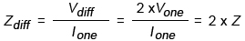 .
.
In this formula, Z refers to the transmission impedance of each signal line, having crucial effect on communication distance and noise resisting ability. Here DM9000 is picked up to transmit differential to network TP_E_TX+ and TP_E_TX-. In order to reduce the effect of reflection, a resistor of 100Ω is placed parallel at signal lines with through-holes applied.
c. Power integrity design of this system
Figure 6 is a basic power distribution model in which current is transmitted to each carrier through power layers and then to ground layer.

In the process of high-speed PCB design, the energy consumption in each unit has to be calculated in the circuit system with the width of power network correctly distributed and suitably amplified.
The power integrity of 6 layers can be summarized as the follows: the maximum pressure drop is 2.1mV, close to 0.06%; the maximum density of current is 16.3mA/m²; within a suitable category, if the density of current surpasses 50 mA/m², the temperature of PCB will rise, which influences the main chip and signal lines in the process of operation. The increasing of copper width is capable of decreasing the current density and increasing the thickness of signal leads is helpful to the decreasing of the temperature of PCB.
d. System electromagnetic compatibility analysis
Electromagnetic interference is usually transmitted as a carrier with useful signals in the way of coupling. In this design, Hyper Lynx simulation software is applied to analyze the radiation intensity of PCB after preliminary design. The crucial signal line, D4, is picked up between ARM9 and SDRAM with probe positions 3m and 10m respectively. Under the situation of excitation source of 220MHz, both FCC and CISPR international standard simulation data can be obtained, displayed in Figure 7 below.

Based on simulation result, the short distance to PCB leads to high radiation from circuit board and the radiation changes with the change of signal frequencies. In the process of high-speed circuit design, PCB anti-interference can be optimized while the noise radiation has to be reduced.


