As far as high-speed electronic systems are concerned, the success of printed circuit board design directly leads to the high problem solving in Electro Magnetic Compatibility (EMC) system in both theory and practice. In order to reach the EMC standard, high-speed PCB design is facing great challenges so high-speed PCB designers must abandon traditional design philosophy and approaches in their process of design. This passage mainly analyzes the misunderstandings and strategies in the process of high-speed PCB design from the perspective of practice.
Dielectric Constant of High-Speed PCB Material
Up to now, there are mainly three design techniques in terms of high-speed PCB design: noise and delayed PCB graph design technique, impedance and propagation delay time control technique and evaluation technique with PCB impedance as parameters among which the latter two types of techniques are the heart of PCB fabrication. There are also a lot of techniques on high-speed PCB fabrication transmissions and the commonly-used basic structures are microstrip and strip line. As to high-speed PCB transmission lines, Z0 that is the impedance parameter and tpd that is propagation delay time are the most important variables. Actually, if the structure of microstrip is different from that of strip line, the calculation formula will also be different. However, in any case, impedance is always the geometric structure of transmission line. In most situations, dielectric constant of part of PCB material is influenced by frequency, area water absorption rate, temperature and electrical characteristics. For two-layer or multi-layer PCBs, their dielectric constant is influenced by proportion of resin and silicon in the PCB material.
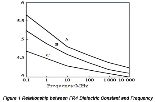
Nowadays, the most commonly-used PCB material is FR4. Usually, PCB material suppliers indicate the values of dielectric constant based on which project technicians will use the material. In the practical applications, the value parameters are usually obtained under the situation of 1MHz while in terms of high-speed situations, dielectric constant has obvious changes as shown in Figure 1.

The three curves in Figure 1 refer to the different proportions of silicon and resin. Among the three curves, curve A is the highest, B medium and C the lowest. Once operators fail to notice the difference, great deviation may take place between calculations or simulation result and practical situations on impedance and propagation delay time, which will have effect on high-speed system signal integrity design.
90° Corner Problem
90° corner should be avoided in PCB routing in most documents because it will possibly lead to impedance discontinuity and Electro-Magnetic Interference (EMI) radiation. From the perspective of theory, the width change of 90° corner is comparatively large, which results in the big impedance and serious impedance discontinuity. From the perspective of practice, the electromagnetic power tends to gather at the corner of routing and the more pointed the corner is, the more gathered power is. Based on the analysis above, the EMI radiation becomes the most protruding at 90° corner.
But some researchers find that the influence of 90° corner on impedance is within 10%. For the routing width of 6mil, if it becomes a key length, then it'll be in the THz range. So, it can be estimated that 90° corner will definitely lead to impedance discontinuity in the practical situations.
Therefore, in the practical PCB routing, at least within the GHz range, it's unnecessary to avoid 90° corner at a cost.
20-H Principles
Since the appearance of 20-H principles by KNG, it has been accepted as the main principle for high-speed PCB design. Even some researchers indicate that this principle is capable of helping ambient electro-magnetic density on concerning PCB layers to decrease by approximate 70%. Besides, it also plays an effective role in reducing the outward EMI radiation. However, lots of experiments don't support the researchers' expectations.
Some experiments indicate that for two-layer PCBs, 20-H principle leads to more serious radiation while for multi-layer PCBs, the utilization of 20-H principle in the inner medium layer doesn't bring about obvious improvement.
Filtering Capacitance Parameters
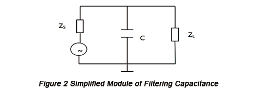
Filtering capacitance is a tested effective and economical measurement used to solve EMC problem in the electronic system. However, high-speed electronic system brings about new requirements to the performance and applicable design of filtering capacitance. The simplified module of filtering capacitance is shown as Figure 2.

It has to meet the following requirement: ZC< ZS// ZL (ZC=1/2πfC). A common misunderstanding indicates that as long as ZC is less than ZL, the purpose of filtering capacitance can be achieved. In fact, parameters of filtering capacitance can't be determined unless the values of ZS and ZL are decided.
However, in high-speed circuit, neither ZS nor ZL is pure resistance, in need of complex values. Meanwhile, ZC isn't pure capacitance in the high-speed circuit and both equivalent series resistance and equivalent series inductance must be taken into considerations. All of these are all difficulties in the application of filtering capacitance in the high-speed electronic system. Once designers ignore these aspects, obvious differences will occur between calculations or simulation result and the practice.
Silicon Packaging
PCB designers tend to pay most attention on PCB layout and interconnections between the components on PCBs and ignore the significance of component packaging. In fact, this will possibly produce serious results to high-speed PCB design. Silicon packaging has influence on silicon's performance through the parasitic inductance, parasitic resistance and parasitic capacitance passing through the connecting lines and lead. These parameters will generate noise, communication delay, edge rate and frequency response. The parasitic parameters of different packaging possibly differ a lot. For the silicon with the same circuit and different packaging, their performances show different features.
In fact, for high-speed electronic system, silicon design, packaging design and board-level design are never independent with each other. For the design flow on silicon, a suitable package must be picked up in accordance with PCB. The overall layout of silicon design is influenced both by techniques and board level elements. For the silicon packaging, its matching with PCB is an element that must be considered. What's more important, a suitable package is greatly helpful in terms of the integrity of board level and EMC/EMI problems. Hence, silicon packaging should never be ignored or despised.
Common-Mode Current Radiation Interference
In the signal transmission leads of PCB, there exists differential-mode current transmitting useful signals and common-mode current without useful information both of which generate EMI radiation.
Because of its relatively high current, differential-mode current has been emphasized by circuit designers with the formation of theory and techniques controlling differential-mode current EMI radiation. As a result, some EDA tools have functions of differential-mode current EMI radiation simulation and prediction. However, compared with differential-mode current, common-mode current is much less, easily leading to the designers' ignorance of common-mode current EMI radiation.
Nevertheless, according to recent research, although common-mode current is much smaller than differential-mode current, the EMI radiation interference generated by the former is much larger than that by the latter. Up to now, common-mode current EMI radiation has become one of the main interference sources of radiation on high-speed advanced circuit boards. What's worse, the generation of common-mode current EMI radiation has seen complicated reasons and neither simulation nor prediction can be achieved. Besides, the research on controlling common-mode current EMI radiation is still on the way.
Therefore, when design high-speed PCB, it's unreliable to simulate and predict EMI radiation based on differential-mode current EMI radiation only.


