


PCB successfully added to your shopping cart
Differential Isometric Processing and Simulation Verification of High-Speed PCB Design
Signals transmitted in differential signal lines contain differential mode component and common mode component of signals.
The amount of differential signals refers to the difference between two signals following formula Vdiff = V1 - V2. The amount of common mode signals refers to half of the sum of two signals following formula 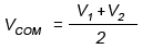 . Therefore, the voltage change of a single line definitely leads to the simultaneous influence on differential mode signals and common mode signals. Next, graph software is applied to draw math function diagram to respectively study the influence on differential mode signals and common mode signals. For convenience of research, signals can be analyzed by simulating them into trapezoidal waveform with the same upper time and down time.
• Influence on differential signals
The positive phase terminal signal, negative phase terminal signal and differential signal of differential line pairs are displayed in Figure 1 below in which full line stands for differential signal wave.

If a phase placement takes place from positive phase terminal to negative phase terminal, there will be a change of difference between positive phase terminal signal and negative phase terminal signal at the up or down edge and this change will change with the change of phase. Tr is used to stand for the shorter time among rising and decreasing time. It can be indicated that when the phase placement is less than point two of Tr, signal distortion is relatively small and the increasing of phase placement leads to strong distortion of differential waveform. When phase placement exceeds Tr, non-monotonic area will take place on waveform. Here the non-monotonic area is a straight line. However, for practical signals, because of reflections, large ups and downs may take place in non-monotonic area with interference pulse formed leading to false triggering, which should be avoided. In addition, the upper edge of differential waveform becomes slow with the increasing of phase placement, which may lead to insufficient establishment time for data signal and may lead to insufficient holding time for clock signal.
• Influence on common mode signal
The phase placement of single terminal signal won't have influence on differential waveform but change the waveform of common mode signals. When phase placement takes place at the positive terminal signal, wave change will take place to common mode signals. It can be indicated that the fluctuation range is related with the amount of phase placement. When the amount of phase placement is respectively 0.05Tr, 0.1Tr, 0.2Tr and 0.5Tr, the fluctuation range of common mode is respectively 5%, 10%, 20% and 50% of the original fluctuation range. When phase increases to Tr or more, the fluctuation will increase to approximately 100% that is the highest fluctuation range. The change of common mode signal may lead to EMI problem and since common code signal isn't received at the terminal under lots of conditions, reflection will form at the receiving terminal, leading to signal ringing. Therefore, the fluctuation range of common mode signal should be decreased as much as possible.
In conclusion, too large relative delay between differential pairs may cause false triggering of signals, signal reflection, EMI and time sequencing problems. However, the influence degree of relative delay signal depends on the scale factor compatible with signal Tr. When the scale factor is 0.05, distortion of differential signals can be almost ignored. However, for common mode signals, when the scale factor is 0.05, voltage fluctuation of common mode signals can be controlled at approximately 5%. Then, even in the situation of full reflection, the reflection voltage stacked on signal lines is just 10% of original fluctuation, which is usually an acceptable value. Therefore, in the process of high-speed PCB design, relative delay of differential signal line in the routing regulation rules can be set to be 0.05 Tr that is capable of meeting the requirement of signal integrity.
Determination of Relative Delay Category
Based on the analysis above, the key of determination of differential isometric category, that is, the determination of relative delay of differential pairs, lies in determination of Tr referring to the smallest value among upper and down time of differential signals. The output of rise time and fall time is actually the output of combination of impedance and capacitance. Therefore, the rise/fall time without loading is actually inherent rise/fall time.
The following three methods can be applied to obtain the value of Tr:
• Rise/fall time can be directly obtained from component manuals. However, in most situations, this parameter isn't provided.
• Value of Tr can be obtained from Ramp keywords from component IBIS (Input/Output Buffer Informational Specification) model. Rise/fall time parameters under Ramp keywords are generally measured at output port connected with a resistor of 50Ω, which are usually 20% to 80% of final voltage time. Since the parameters are obtained without considering the influence of package, it's strict for us to use rise/fall time as the value of Tr.
• The value of Tr can be estimated according to the minimum clock frequency or maximum clock frequency of output signals. Because distributive rise edge is approximately 10% of clock frequency in most high-speed digital systems, the value of Tr can be estimated with the minimum clock period Tclk provided based on formula: Tr = Tclk x 10%.
The estimated value obtained through clock period is usually strict because package parasitic parameters or loading of components will make the inherent rise/fall time in transistors greatly slowed.
In the practical work, in most situations, circuit designers don't provide information of Tr to PCB layout engineers who only receive some ambiguous demands in terms of differential isometric control. The third method undoubtedly provides a simple scheme to PCB layout engineers as long as the highest clock frequency on the signal line is obtained. The highest clock frequency is regarded as the most reliable design parameter for circuit designers and it is usually supplied to PCB layout engineers at the beginning of PCB design.
The third method usually leads to a list of reference values within relative delay control category between differential pairs, as shows in below table.
| Clock Frequency/ns | Clock Frequency/MHz | Relative Delay Category/ps | Transmission Line Length/mil |
| 3.75 | 266 | 18.8 | 105 |
| 3 | 333 | 15 | 84 |
| 2.5 | 400 | 12.5 | 70 |
| 1.87 | 533 | 9.4 | 52 |
| 1.5 | 667 | 7.5 | 42 |
| 1.25 | 800 | 6.3 | 35 |
Simulation Verification
Take DQS (Data Strobe) differential signal between TSM320 and MT41J256M16 as an example, Cadence simulation software is applied to transmit DOS signal to DRR3 memory to simulate memory control chip, analyze its influence on data signal establishment holding time and verify the analysis above. Simulation circuit is shown in Figure 2 below.

Based on Figure 2, the reference voltage of output pins is 1.5V; memory control chip is directly connected with memory chip through ODT (On-Die Termination) mode with transmission line of 800mil; differential impedance is 100Ω and simulation clock frequency of 800MHz. A transmission line of 50Ω is serially connected with DQS positive phase terminal to simulate discrepancy phenomenon of differential pairs. In the situation of isometric differentials, the length of single-terminal transmission line of 50Ω is 0mil.
Simulation is carried out to the differential isometric circuit. Figure 3 illustrates the output signal at the positive phase terminal of differential signals. Through measurement, the rise time is approximately 216ps while fall time 219ps so the minimum rise/fall time Tr should be 216ps.

Figure 4 is an eye diagram of data signal DQ and gating signal DQS through simulation with the establishment time 205ps and holding time 337ps. According to the turnover rate of DQS and DQ signals through simulation and based on data manual, the minimum establishment time of data signals by receiving terminal is required to be 85ps and the minimum holding time is 95ps. Therefore, the overmeasure of the minimum establishment time is 120ps and holding time 242ps.

The situation of the existence of 0.05Tr phase placement, 0.2Tr phase placement and 0.5Tr phase placement at the positive phase terminal has to be considered. The circuit can be simulated with single-terminal transmission line length that is respectively set to be 60mil, 240mil and 600mil. Differential signal waveform and common mode signal waveform through simulation for 4 times are illustrated in Figure 5 and 6.

Based on Figure 5, distortion is the minimum when relative delays of 0.05Tr and 0.2Tr take place. Especially when relative delay is 0.05Tr, only placement of about 5ps from differential signal to differential signal waveform with no relative delay so that the data signal establishment over-measure is increased by about 5ps with holding over-measure time decreased by 5ps. Although holding over-measure time is decreased, this amount of placement is so little for the holding time of 242ps. Time sequencing can be avoided. For the situation when relative delay is 0.5Tr, the placement of DQS signal waveform has reached about 60ps. Although this placement is still within the category of over-measure, sufficient attention should be paid.

Based on Figure 6, the increase of phase placement leads to obvious periodic fluctuation on waves and the gradual increase of range. When the relative delay is respectively 0.05Tr, 0.2Tr and 0.5Tr, the measured peak value of common mode signal is respectively 61mV, 176mV and 430mV among which the highest value is seven times of the lowest. The largest fluctuation range is respectively 4.3%, 12% and 29%.
In conclusion, simulation result is compatible with the result obtained through math function diagram analysis. When the relative delay between differential pairs is less than 0.05Tr, the influence on signals is quite small.
The minimum clock period of output signal at output terminal is applied to estimate the relative delay control category. Based on component manual, the minimum clock period of components is 1.25ns with clock frequency of 800MHz. According to Table 1, relative delay should be controlled within 6.3ps with transmission line length of 35mil. Apparently, this value is much smaller than the control category of the relative delay of 0.05Tr through simulation. Therefore, the estimated relative delay control category is relatively conservative, which is more specific than the simulated result.
Helpful Resources
• Research on High-Speed PCB Design in Embedded Application System
• How to Design Image Planes for High-Speed PCBs
• High-Speed PCB Design Challenges on Signal Integrity and Their Solutions
• Simulation PCB Using OrCAD PSpice
• Full Feature PCB Manufacturing Service from PCBCart - Multiple Value-added options
• Advanced PCB Assembly Service from PCBCart - Start from 1 piece