Nowadays, multilayer PCBs are used in most high-speed circuit systems and lots of circuit systems have numerous operating powers, providing strict requirements to image planes design, especially the settlement of relationships between multiple power/ground planes. Besides, special copper clad surface needs to be designed on device layer design in order to stop oscillators from producing RF (radio frequency) energy and provide excellent heat dissipation for high power components.
Functions of Image Planes
Image planes are a copper clad surface adjacent to signal layers in printed circuit boards. The main functions of image planes include:
1). Reducing reflow noise and EMI (Electro Magnetic Interference). Image planes provide paths with low impedance for signal reflow, especially when large current is flowing in the power distribution system. What's more, ithey decrease the closed ring area formed by signal and reflow so that EMI goes down.
2). Controlling crosstalk between signal lines in high-speed digital circuit. Crosstalk is determined by the ratio D/H in which D refers to the distance between interference source and interfered object and H refers to the height of image planes between signal layers. The ratio D/H can be controlled by changing the value of H so that the crosstalk between signal lines will be ultimately controlled.
3). Controlling impedance. The characteristic impedance of printed wiring is related to the width of wires and the height between wires and image planes. If there is no image plane, it's possible that impedance can't be controlled, which leads to the failure of transmission line matching and signal reflection.
Besides, image planes are also capable of controlling the noise from reflection to outer boards. It has to be acknowledged that image planes alone are not sufficient for the implementations of those functions strict design rules must be supplemented to achieve expected targets. This fact can be put as: in order to control noise in high-speed digital circuit, image planes are essential but they can't work alone.
Layer Skipping of Signal Reflow
In multilayer PCBs, each layout layer should be adjacent to one image plane and the returning circuit of signal flows on the corresponding image plane. When a signal line isn't passing through a layout layer, the ordinary method is that first signal line is connected to a layout layer and then the signal line is connected to another layer by through holes. Therefore, signal line is skipping from one layer to another, so is returning current following the same path. When both the layers are ground layers, returning current is capable of skipping by through holes connecting two layers or ground pins. When one layer is power layer and the other is ground layer, returning current's only opportunity of skipping between layers is the position with decoupling capacitor placed. If there is no decoupling capacitor or through holes connecting the ground layer, skipping must be made by returning current that has to follow the farthest way, which makes returning current decoupled with other circuits so that crosstalk and EMI will be caused.
As a result, in the process of PCB design, layer skipping should be set at the ground pins adjacent to components or around decoupling capacitor at best. When this can't come true, ground through holes (skipping between two ground layers) or bypass capacitor (skipping between a power layer and a ground layer) can be placed at the skipping point in order to make returning current skip.
Splitting Planes
In the process of using multilayer PCBs, sometimes it's necessary to generate an area without copper foil with certain width, splitting an integrated image plane into several independent parts, which is called splitting planes.
Splitting planes is usually used to stop noise interfering sensitive circuits and isolate different reference voltages such as stopping digital noise entering analog, audio, I/O area and isolation between 5V and 3.3V power voltages.
Splitting planes can be classified into complete splitting and incomplete splitting. The former refers to the complete isolation between power layers and ground layers after splitting. The latter refers to the complete isolation between power layers while ground layers are connected by "bridges". Whether to use complete or incomplete splitting depends on whether there's signal connection between splitting planes.
• Examples of splitting planes
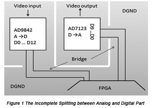
Figure 1 is part of image planes design of analog and digital mixed circuit of a test platform. Video analog input is transmitted to FPGA by the conversion of AD and output as DA conversion. Both AD and DA use independent power component for providing power. Digital components account for most of the space of the board while analog components only account for a small part. However, all of them are essential parts that are important for the performance of the whole system. Therefore, much care must be taken in the process of dealing with those components. It's ideal that the noise of digital part doesn't enter the analog part. However, some signals from AD and DA converters are connected to FPGA of digital part. In order to ensure the reflow of these connected signals, digital power and analog power must be completely isolated while digital ground and analog ground must be incompletely isolated so that the influence of analog part from digital part is decreased to the minimum.

All the lines from digital part to analog part must pass through the bridge whose opening size should be just suitable for the passing of required wires so that data signal reflow will be capable of returning by the bridge, avoiding the interference to other signals as a result of winding for returning path. In this PCB design, grounds of AD and DA part are completely isolated from each other.
• Some problems in the process of splitting planes
a. Overlapping of isolation layers
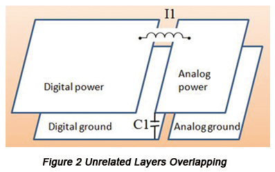
In the multilayer PCBs, splitting planes are usually used to isolate different powers. Generally speaking, the corresponding ground layers of these powers are isolated with each other, that is, each power has its own reference layer. In the process of PCB design, overlapping of isolation layers must be avoided. For example, in most multilayer PCBs, the power and ground layer of analog part and digital part are isolated with each other. Analog power layer and digital ground layer mustn't be overlapped in space just like Figure 2.

If an overlapping isolation layer appears, a small pad capacitance C1 will appear in the overlapping area. The capacitance will make RF energy transmitted from one layer to another isolated, static and independent layer to decrease the validity of isolation.
b. Decoupling capacitor placement
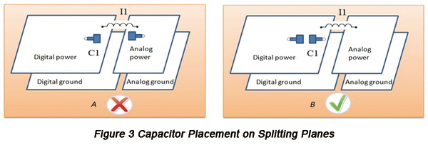
To filter the noise with high frequency generated by high-speed components, lots of decoupling capacitors are arranged on PCBs. If splitting planes come out in PCBs, in the process of layout a situation will possibly take place that ground pins of decoupling capacitor aren't connected with other reference ground layers instead of the corresponding ground layer. This type of mistake will possibly take place and leads to the noise decoupling from one layer to another, which is similar with splitting planes overlapping. That's why this problem should be dealt with in the stage of design. Take digital analog mixed circuit as an example again. Analog power is brought in from digital part through ferrite bead and C1 refers to the decoupling capacitance of digital part. In Figure 3A, power pins of C1 are connected with digital power while ground pins with analog ground, leading to the decoupling of digital noise with high frequency in sensitive analog part, which is a wrong connection. Figure 3B is a right decoupling capacitor connection.

c. Single point grounding
When reference layers of different powers are connected together, single point grounding must be ensured. In the exemplified digital analog mixed circuit, circuit boards are classified into digital part and analog part and both digital ground and analog ground have at least two connection points so that noise signal possibly forms circulation between two reference layers through the two connection points, which is called "ground loop". Ground loop will lead to noise, EMI, energy consumption and heat dissipation difficulty. There's an easy solution to the problem of ground loop: as long as there's only one connection point between reference layers, loop can't be formed.
Local Ground Layers
As a part of image planes, local ground layers refer to a copper clad on the top surface of PCBs, directly connected with the inner ground layer. Its main function is to capture RF magnetic flux generated by the inside of some key chips (oscillators for example) or to be used for power dissipation.
To obtain excellent performance, oscillators, crystals and clock supports should be assembled on an independent local ground layer. The reasons include:
1). If the oscillator is packaged in a metal clad, RF current generated inside the metal clad will possibly be so large that its ground pins fail to lead the large current to the ground with a method of low energy consumption. As a result, this metal clad becomes a unipolar antenna.
2). If surface mount assembly technique is used when placing the oscillator on PCBs, the problem mentioned above becomes worse since plastic material is usually used in SMT packaging, stopping RF current led to the ground point. Finally, RF current generated inside the packaging will be radiated into the free space and decouple with other components.
3). Ordinary oscillators are capable of driving clock buffering that belongs to components with super high speed and fast edge rate, producing a large amount of RF current, which will possibly lead to current function failure.
If a local ground layer is assembled in the oscillator and clock circuit, image planes will be provided, used to catch the RF energy generated in the inside of the oscillator and corresponding circuits so that RF radiation can be decreased.
20-H Rule
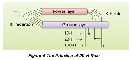
As an empirical rule, 20-H rule describes that in multilayer PCBs with high density, in order to reduce electromagnetic energy radiated to free space by circuit boards, the size of power layer should be smaller by 20H than that of ground layer in which H refers to the distance between the two layers. In Figure 4, the left part indicates the power/ground layer without any special design in which the edge radiation is so strong that it will influence the functions of adjacent circuit. The right part indicates the RF radiation situation through decreasing power surface size by X-H. It can be seen that ground layer attracts lots of magnetic lines of force and RF radiation energy is decreased. According to the result of experiments, RF radiation force begins to go down from 10-H; in the case of 20-H, ground is capable of attracting 70% of magnetic flow; in the case of 100-H, magnetic force is capable of decreasing by 98%.

Naturally, 20-H isn't perfect for all PCB structures. The efficiency of 20-H depends on the operating frequency, physical size of power/ground layer and the distance between them the latter two elements of which decides PCB board's SRF (self-resonant frequency). Research indicates that when PCB operates at any SRF, 20-H doesn't work and ground fails to attract radiation energy as well. What's worse, lots of radiation energy will be generated instead. Therefore, in the practical high-speed circuit, specific situations must be taken into consideration when deciding whether to choose 20-H rule or not.

