LED (Light Emitting Diode) display has been embraced by electronic industries owing to its merits ranging from high lightness, low energy consumption, long lifetime to stability. Due to the constant progress on technical indexes like pitch, stability, lightness or color depth (grayscale), printed circuit boards (PCBs) have to meet increasingly higher requirements in terms of quality and reliability of end products.
LED PCB Manufacturing Setbacks
• Circuit Graphics
Because circuit lines and pads are arranged in high density on LED side, scratch reduction is the upmost consideration during fabrication. It is suggested to design dense circuit layer according to reference picture as exposure is being implemented. Efforts have to be made to decrease polishing scratch and image defects in the process of board polishing in via filling process (VFP) and board polishing prior to solder mask application.
• Contour Tolerance
Current contour tolerance of LED boards is usually at ±0.1mm. However, more rigorous tolerances like ±0.08mm or ±0.05mm tend to be required based on necessity during LED display assembly. Therefore, mechanical manufacturing of LED circuit boards have to be confronted with large challenges.
Moreover, striving for high utilization of panels leads to limited technical margins in PCB fabrication process. Furthermore, only a couple of small thru holes are allowed in the board with a number of 3 to 4 and diameter approximately 0.8mm. As a result, screws fail to play a role of fixation that should do in the procedure of milling so that it's possible for issues to take place including figure asymmetry, board angle bulge, and solder mask oil peeling. When a board features a normal figure size, problems are often caused such as inconformity between via and margins, pad and margins.
• Solder Mask Color
Solder mask color is a significant parameter to determine prior to PCB manufacturing and there are lots of selections from traditional colors including green, red and black to unusual colors such as matte black or purple representing personalities. Nowadays, matte black is mostly applied by LED circuit boards and solder mask color differentiations between circuit boards in different batches are closely associated with resolution of LED display. When LEDs feature large enough pitch between each other, solder mask color differentiations can be compensated by lampshade. However, the reduction of LED pitch leads to constant failure of lampshade so that LED side will be directly exposed to outside. Moreover, solder mask color differentiations can be aroused by copper layer processing prior to solder mask, solder mask thickness, exposure differentiation and waiting time for solder mask to solidify.
• Electrical Test
No-margin design of LED PCB greatly challenges marking-up in electrical test as well. Size and LED pitch of an LED circuit board directly determines the number of LEDs and pads. Up to now, it usually occurs that the number of LEDs on LED side of a circuit board exceeds decades of thousand and that of pads exceeds 60 thousand. Such a high density of LED arrangement brings extremely heavy difficulties to the running and termination of electrical test. Therefore, multiple electrical tests or flying probe test have to be relied. Nevertheless, flying probe test features a disadvantage of much time consuming.
LED PCB Design Techniques
In spite of the listed PCB manufacturing setbacks, together with attributes of LED PCBs like small pads, large number of pads circuit with high density, some methods are available to overcome those setbacks through PCB design.
• Pitch
PCBs applied for LED display, also called LED PCBs, are highly symmetrical in outer design. When it comes to copper layer of LED circuit boards, one side is fully covered with pads that are arranged in matrix, called LED side. Generally speaking, 4 pads are regarded as one unit on which an LED is assembled. Components are assembled on the other side of copper layer, which is called driver side.
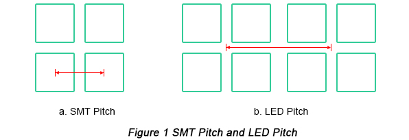
The smaller LED pitch is, the better display effect will be and so will be its resolution. Up to now, the pitch range in harmony with current SMT (Surface Mount Technology) is from 0.45mm to 1.6mm while LED pitch is from 1.0mm to 4.0mm. LED PCB design mainly depends on specifications of LED pads. The figure below indicates comparison between SMT pitch and LED pitch.

• Laser Drilling Blind Vias
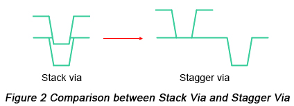
As for stack boards containing 2 layers at least, electrical soldering blind via filling technique is required when stack via is designed as laser drilling ones. Eventually, procedure complexity and manufacturing cost will go up. Thus, when it comes to stack boards with more than 2 layers, laser drilling blind vias are suggested to be designed as stagger vias instead of stack vias. Laser drilling stack vias should try to be avoided.

• LED Installing Holes
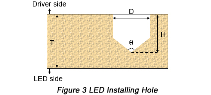
LED installing holes are non-penetrating holes with advised diameters tolerance at ±0.05mm; depth (H) should be no more than the value of board thickness (T) minus 0.5mm with formula: H ≤ T - 0.5mm. Depth tolerance should be more than ±0.2mm while the conventional drilling angle (θ) is 130°. Figure 3 shows parameters of an LED installing hole.

If copperless area around non-penetrating (NP) holes features insufficient distance, NP holes will possibly be plated thru-holes or copper will be exposed at the margin of vias. When it comes to NP holes requiring solder mask opening pad to be left on the surface of vias, copperless separation area larger than 0.15mm should be designed between NP vias and pads. When NP vias need no pads, the whole pad can be cancelled.
• Distance between Pad and Outer Margins
Sufficient space has to be retained between margin pads and outer margins. If space is insufficient, issues like milling detects & copper exposure will occur.
• Solder Mask Opening Pad
Copper define is suggested on pads, which is capable of effectively stopping solder mask peeling. When SMT margin pitch is rightly fit for manufacturing, SM define can be considered. As a result, pads will share high level of conformity.
8 Methods to Overcome LED PCB Defects
• Circuit Scratch
Pads in high density on the side of LEDs lead slight scratch to be a deadly defect. It's suggested that relatively high volume of copper foil should be applied so that open and short circuit scrap will be definitely reduced caused due to scratch.
Along with the features of larger window techniques, pads in high density lead to recessive defects of copper exposure at the side of circuit. This type of defects is seldom observed until SMT procedure has been completed. This problem can be partly solved by relatively shrinking line pitch to improve pitch between line and pad.
• Solder Mask Oil Peeling
Black solder mask lays high requirement to exposure energy and even slightly thicker solder mask oil can easily lead to incomplete exposure of solder mask oil at the bottom layer, finally causing solder mask oil peeling. Secondary exposure can be applied to effectively solve this problem. Of course, solder mask consignment capacity will be challenged as well.
• Solder Mask Oil Color Inconformity
Distinct with most printed circuit boards, LED side of an LED circuit board features high requirement to color inconformity. Until now, there are no judging standards accepted by the public and it is extremely difficult to judge it in quantifications. Oil color conformity results from a large number of elements. Furthermore, it depends on stricter manufacturing conditions than ordinary circuit boards. Therefore, oil color conformity can be achieved by exploring the most suitable control parameters and methods, which calls for rigorous manufacturing technologies and years' fabrication experience in this industry.
• Bad Board Outline
As for smaller boards without margins, LED installing holes lead to bad marking up effect and marking-up screws tend to be loose and displacement, causing defects such as outline displacement and board angle bulge. Suitable process assistance margins can be selected as an improvement method.
• Board Angle Defects
When it comes to circuit boards with relatively high thickness, fragile side angles on LED circuit board should receive carefulness from operators. In order to avoid defects in the process of transportation, it's necessary to add base plate for protection as a protection measure. Plus, size of the base plate should be a little larger than that of single margins.
• Warpage
LED side of an LED circuit board contains a large number of pads in high density while large blocks of copper are arranged on the driver side. This type of asymmetrical stress is regarded as the main reason contributing to board warpage. In order to maintain reasonable flatness, warpage of LED board has to be rigorously controlled within under 0.5%.
• Pad Outline
Pad arrangement in matrix type easily lead to visual inspector's visual fatigue, which causes a high omission ratio. Nevertheless, outline inspector features problems such as long inspection time and low pass rate. Therefore, those issues can't be efficiently reduced unless efforts are made on procedure control.
• Degrading Functions
Distinctions between other types of PCBs and LED PCBs, black solder mask and pads in high density bring about difficulties to error analysis of printed circuit board assembly (PCBA). When bad functions occur, PCBA only describes them and fail to indicate which specific pad. This problem is usually demonstrated as failure of the whole row of LEDs. Confronted with such issue, specific network dot should be determined after lots of efforts. The optimal method to make it true should depend on concerning components demolition and solder mask oil removal.

