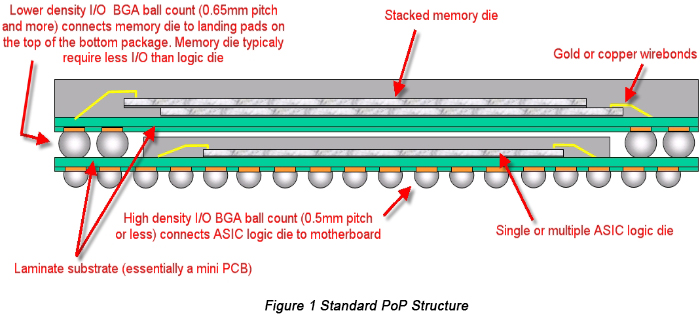
There're two widely used PoP structure, namely Standard PoP Structure and TMV PoP Structure.
Standard PoP Structure
In a standard PoP, logic devices are placed at the bottom package and logic devices feature a structure of fine pitch BGA solder in harmony with device's attribute of a large number of pin counts. The top package in the structure of a standard PoP contains memory devices or stacked memories. Owing to insufficient pin counts memory devices contain, margin array can be applied so that interconnections between memory devices and logic devices at the margin of two packages.
Currently wire bonds are fast being replaced by flip chip technology in bottom package to meet higher demands of smaller package size, which cause solder pitch in bottom package constantly going down. 0.4mm solder pitch has been commonly applied in bottom package. Moreover, both dynamic random-access memory (DRAM) chip and DRAM chip containing flash memory in upper package strive for higher speed and bandwidth. Correspondingly, top package should have more solders, which make it necessary to reduce solder pitch of upper package. Initially, a pitch of 0.65mm was far sufficient while finer pitch is currently required. Just like what was mentioned just now, a pitch of 0.4mm has been widely applied in PoP structure.

Image from wikipedia.org
Miniaturization through high integration is the key element contributing to wide popularity of PoP. Leading elements determining PoP size include:
• Maximum size of a bare logic device;
• I/O interface counts for logic devices;
• Overall bus count of power and ground;
• Dimensions of memory devices in upper package that provide overall I/O, power, ground and mechanical support;
• High-density wiring and cross network required by configuration of logic and memory devices integrated in BGA;
• The overall solder count demanded by bottom package and concerning area.
TMV PoP Structure
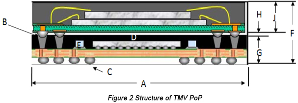
Through mold vias (TMV) PoP, a creation and improvement based on standard PoP, has been widely applied in handheld electronic applications owing to its merit of fine pitch. Figure 2 displays the structure of TMV PoP.

The following table indicates the leading dimensions of a structure of TMV PoP.
|
Package (A)
|
Upper solder
array (B)
|
Bottom solder
array (C)
|
Silicon wafer (D)
|
Passive
component (E)
|
Stacked package (F)
|
| 14*14mm |
Pitch: 0.5mm
Pads: 200
Array: 27*2 |
Pitch: 0.4mm
Pads: 620
Array: 33*6 |
7.10mm*6.97mm*0.13mm |
Size: 0105
Quantity: 32 |
Through mold top: 0.40
Under layer: 0.21mm
Bottom package height: 0.76mm
Clearance (H): 0.03mm
Top package height (J): 0.53mm
Overall height: 1.32mm |
In a TMV PoP, through mold vias are responsible for electric connection between logic device in top package and memory device in bottom package which is achieved by through mold vias in bottom package and between top solder in bottom package and solder in top package. Both solders in top package and bottom package were spherical solder prior to soldering after which they became cylindrical objects B points to like those in Figure 2.
TMV PoP is expected to be capable of shrinking package size, thickness and warpage. Moreover, it allows the next generation of PoP to achieve higher interconnection density, performance and reliability. Its advantages include:
• Broke bottleneck between pitch and package clearance, help meet demands of increasing memory interface density.
• Balanced fully-molded structure is beneficial to warpage control so as to meet the demand of reducing bottom package thickness.
• Dimension ratio is added between chip and package.
• Contributive to configuration of wire bonding, FC, stacked chip and passive component.
• Help increase reliability of top components and bottom through mold vias are capable of holding solders with larger volume, supporting larger stand-off height and improving stress distribution of thermal cycling.
When it comes to surface mount technology (SMT) modes of PoP, two types of technologies are available: pre-stacked PoP and on-board stacking PoP.
In pre-stacked PoP technique, manufacturers will stack top package and bottom package, carry out soldering to make the combination be a component that is called pre-stacked device, then attach the combined component to printed circuit board (PCB) surface and implement reflow soldering.
In on-board stacking PoP technique, manufacturers will sequently stack bottom package and top package on circuit board. First, they will mount bottom package on circuit board, then mount top package on bottom package after dipping into flux or solder paste. Next, conduct a reflow soldering on the stacking package.
Take a double-side SMT assembly as an example, steps of on-board stacking PoP assembly include:
• Non-PoP side component assembly (printing, mounting, reflow soldering and inspection);
• Solder paste printing on PoP side;
• Bottom package and other devices mounting;
• Top package devices dipping flux or solder paste;
• Top package mounting;
• Reflow soldering;
• Inspection (X-ray or AOI).
Compared with pre-stacked PoP SMT assembly technique, on-board stacking PoP contains two more steps: top package's flux or solder paste dipping and top component mounting.
Step One: Solder Paste Printing of PoP Bottom Package
Solder paste printing of PoP bottom package is determined by component size, pad size and clearance between components. Wide applications of 01005 and high-density CSP (chip scale package), clearance has developed from 0.1-0.15mm and stencil printing clearance falls in the range from 4-5mil. To meet such increasing requirement, laser-cut and/or ladder stencil template by electroforming is usually applied. Solder paste is selected based on printing clearance. Many companies start to use Type IV solder paste while Type III solder paste is still applied in many situations.
Bottom package of PoP assembly is the same as BGA (ball grid array) and CSP assembly in terms of solder paste printing control technique so no remarkable differentiations have been found between bottom package PoP and other fine-pitch components. Printing quality inspection can be achieved with printer or AOI (Automated Optical Inspection) equipment.
Step Two: PoP Top Package Dipping
Either solder paste dipping or flux dipping, all mounting systems have to consider integrated dipping module so as to successfully achieve top package dipping. During dipping, the overall dipping capacity has to be considered. With the improvement of contact area, stress brought by PoP to the surface of solder paste goes up correspondingly. To avoid insufficient or incomplete solder paste picking, it's recommended to modify absorbing capacity or the area where an absorbing tool works. Prior to surface mounting assembly, any transverse movement between solder paste surface and PoP stacking will definitely contribute to possibility of badly-performed wettability on soldering ends. Solder paste has to be eliminated that is peripheral to soldering ends prior to reflow soldering, or soldering defects might be caused.
It's significant to closely observe the changes of solder paste surface after dipping. Solder paste thickness is controlled by scraping blade that moves hard on the surface of solder paste.
After dipping and before surface mounting, positioning inspection system owned by surface mounting equipment should be able to inspect solder paste or flux draining and insufficiency on solders and to inspect excess solder paste on solders as well. Unsuitable dipping thickness or solder paste viscosity changes possibly lead to changes of dipping solder paste volume. Furthermore, owing to environmental changes, long waiting time in a tray and time of exposure to time possibly drive changes in terms of attributes of solder paste.
Great challenges to solder inspection after dipping and before surface mounting occur due to color recognition issues. Some visual modifications can be seen on solders after flux dipping when it comes to PoP and FC. To meet AOI demands, flux suppliers must color flux. Currently, colorants such as white, black and red are widely applied in flux.
Both solder paste dipping and flux dipping have to rest assured that reliable volume of solder paste or flux can be achieved. When it comes to specific applications, experiment or optimization can be relied but for issues that fail to be evaluated, other methods should be explored. For example, it's relatively a hard job to judge the volume of dipping flux and volume of solder paste dipping should be evaluated through observations of weight modification after dipping.
To obtain excellent dipping effect, a couple of significant elements have to be ensured by solder paste dipping and flux dipping, including: homogeneity, staying time on a tray, consistency between dipping amount and volume, and waiting time prior to reflow soldering after dipping.
A. Homogeneity
Initially, homogeneity was inspected in the way that dipping material was first smeared on the surface of glass and then was observed under an optical microscope. If even creaminess texture was observed, it was indicating that homogeneity was successfully achieved. But if wavy or grainy appearance, large particles and conglomerates were found, it was indicating that homogeneity wasn't achieved. Requirements on homogeneity are determined by size of PoP. Generally, particles whose diameter exceeds one third of that of solder mustn't be mixed in dipping.
B. Staying time on a tray
In the process of dipping, flux or solder paste is evenly distributed on a rotating tray by a doctor blade capable of setting the thickness. Owing to moisture ingression or evaporation, attributes of material will go down or even lead to inconsistency. Staying time should be as long as a whole work shift (8 to 10 hours) and can be calculated by monitoring the consistency of PoP after dipping with dipping equipment. Moreover, viscosity of solder paste and flux can be measured based on regulations of IPC-TM-650 in which printing thickness is stipulated to be in the range from 200-250μm.
C. Consistency between dipping amount and volume
It's a complicated issue to determine consistency between dipping amount and volume, especially for flux dipping. PoP dipping amount can be calculated through measuring its weight before and after dipping.
Dipping solder paste consistency can be inspected under an optical microscope after dipping by inversing PoP. It's such a challenging task to measure consistency of flux dipping due to transparency of flux that the following steps are provided as a guide:
• Place flux in a rotary pool and use a fixed rubber roller to ensure the consistency.
• Pick PoP and dip it into flux.
• Place PoP onto a copper board and then pick PoP to make flux left on the board.
• Observe the copper board under a microscope with a magnification of 45.
Another method to measure the distribution of flux is to stack PoP through flux dipping onto a piece of glass laminate and then to tie them together with tape. Turn the integration over and distribution of flux can be observed. Halo of flux can be directly seen on the glass laminate.
When it comes to flux that has been colored, it's easier to measure consistency of its flux distribution. Nevertheless, volume of dipped flux is so small that coloring method is usually neglected.
D. Waiting time prior to reflow soldering after dipping
Generally speaking, waiting time prior to reflow soldering after dipping lays little influence on soldering quality and even dry flux won't lead to extremely low soldering quality. In many situations, gel flux is sufficient for reliability of solder. But solder paste has a totally different story. Because solder paste powder tends to be oxidized, acceptable waiting time prior to reflow soldering after dipping has to be ensured in advance.
Waiting time identification can be achieved through an experiment in which solder forming is observed, aiming to eliminate oxide prior to solder forming, which helps ensure excellent solder forming. As a result, flux or solder paste has to be tested in extreme environment so as to indicate whether they are capable of maintaining longer waiting time prior to reflow soldering after dipping. Conditions and requirement of this experiment include:
• Flux or solder paste has to be exposed to high humidity.
• Prior to reflow soldering, flux or solder paste has to be exposed to the air for a long time in high temperature. For example, relative humidity should be 95% and exposure time is respectively 2/4/8 hours when performance of flux or solder paste is tested.
• After reflow soldering, solders have to be inspected under X-ray to find defects such as wetting, cavity and bridging.
In this experiment, dipped PoP configuration should be turned over first and then exposed to high temperature and high humidity in order to avoid damaging flux or solder paste that has been dipped on solder.
E. Flux dipping
Flux dipping features three leading advantages: size difference that originally occurs between solders won't be magnified; technique is controllable; material is easy to be picked.
Since chip features a low warpage, application of flux in FC won't lead to open soldering. Perhaps based on the experience of applying FC, dipping flux was initially selected by PoP. However, PoP owns at least two contact surfaces (circuit board and bottom PoP, bottom PoP and top PoP) each of which features potential warpage issues. The solution to this problem lies in flux dipping thickness improvement that may not cause soldering defects but will definitely lead to a larger amount of contaminant, which is possibly a genuine problem for afterward bottom filling.
F. Solder paste dipping
To solve the problem caused by PoP warpage, it's necessary to use solder paste dipping as replacement of flux dipping. Compared with flux dipping, merits of solder paste dipping include:
• Capable of compensating for warpage of components and substrate to some extent;
• Excellently compatible with current techniques without need for extra techniques' participation;
• After soldering, a relatively large distance between component and board is beneficial to reliability;
• Prior to surface mounting, solders with solder paste dipping tend to be inspected more easily.
Although solder paste dipping has been regarded as optimal alternative with quality and performance considered first, it features disadvantages:
• Capable of magnify distinctions between solders;
• Such limited types of solder paste that can be applied and costly.
Type V solder paste or solder paste with smaller particles are suggested to be applied in dipping. Metal content of solder paste should be approximately 80%-85% w/w and application of solder paste contributes to connection between solder and pad, shrinking the possibility of open soldering. As solder paste with tiny particles features a high level of oxidization, application of such type of solder paste can not only improve homogeneity but delay fusion procedure as well.
In the procedure of reflow soldering, because top package of PoP maintains a high temperature, core ingression may take place on solders in spite of existence of solder paste, which perhaps lead to open soldering. When solder paste containing tiny particles is applied, a lower melting speed of solder paste can lead top package and bottom package to simultaneously reach the same temperature so that core ingression can be prohibited.
Thickness of solder paste dipping should be determined by dimensions of component solders to ensure suitably stable and even thickness and make the smallest solder to be dipped by solder paste. Solder paste dipping depth must be rigorously controlled. It is indicated by experiments that when dipping depth exceeds 50% of solder height, on one hand, amount of solder paste will be increased; on the other hand, solder paste will wrap around the ball terminations, leading to excess solder paste deposition, which will possibly bring about soldering defects.
Step Three: PoP Component Positioning
Owing to special structure of PoP, much care has to be taken into top package positioning and control because all advanced surface mounting system has to ensure Z-axis dimensions accuracy control and to withstand shock and vibration in the process of assembly.
Stacking feature of PoP tends to cause displacement. During mounting, random vibration will be caused at times due to stretching of conveyor belt of mounting equipment. Gas convection has to be carefully considered in reflow soldering equipment, as sometimes it can also cause the vibration.
Step Four: Reflow Soldering of PoP
Lead-free techniques tend to bring about defects such as metal oxidation, bad wettability and incomplete solder. In nitrogen with a low concentration of oxygen (50ppm), soldering reduces metal oxidation and performs excellent wettability, capable of contributing to the forming of complete collapse. Moreover, it performs well in self-centering with soldering cost increased by 25%-50%.
Because lead-free soldering features a high temperature, relatively thin components or substrates (thickness could be 0.3mm) are easy to be deformed in the process of reflow soldering, it's necessary to demand delicate and optimized reflow soldering temperature curves. Furthermore, internal temperature of top package components and bottom package ones play such a key role in reflow soldering that surface temperature of top package components shouldn't be too high while solder and solder paste belonging to bottom package component have to be fully melted to be high-quality soldering spots. When it comes to multiple stacking assembly, temperature rising speed is suggested to be controlled within 1.5°C/s to stop some defects from occurring including thermal shock, in-furnace displacement etc. On the premise of soldering quality guarantee, reflow soldering temperature should be as low as possible to decrease possibility of thermal distortion to the largest extent.
It's also worth reminding that due to plastic as packaging material of PoP, humidity of PoP has to be strictly managed to avoid popcorn.
Step Five: Optical and X-ray Inspection of PoP
Many types of defects may occur in the procedure of PoP assembly and soldering, such as Open soldering, Cold soldering, Bridging, Core ingression, Insufficient solder paste, Excess solder paste, Solder cavity, Solder loss, Lifted pads, Pillow defect, Debris, Tin ball, Excess flux, Package warpage, Broken package, Damaged solder mask and Solder mask displacement. Inspection methods help to defeat those defects, including AOI, endoscopic inspection, X-ray inspection, oblique X-ray inspection and 3D X-ray inspection. The following table showcases each method's inspection capabilities based on its attributes.
| Inspection method |
Optical inspection |
X-ray inspection |
| AOI |
Endoscopic inspection |
2D |
2D+oblique view |
3D |
| Open soldering |
partially |
partially |
X |
√ |
√ |
| Cold soldering |
partially |
partially |
X |
√ |
√ |
| Bridging |
partially |
partially |
√ |
√ |
√ |
| Core ingression |
partially |
partially |
X |
√ |
√ |
| Insufficient solder paste |
X |
partially |
X |
√ |
√ |
| Excess solder paste |
X |
X |
X |
√ |
√ |
| Solder cavity |
X |
X |
√ |
√ |
√ |
| Solder loss |
partially |
partially |
√ |
√ |
√ |
| Solder peeling |
partially |
partially |
X |
√ |
√ |
| Pad peeling |
X |
partially |
X |
√ |
√ |
| Pillow defect |
partially |
partially |
X |
√ |
√ |
| Debris |
partially |
partially |
partially |
partially |
partially |
| Tin ball |
partially |
partially |
√ |
√ |
√ |
| Excess flux |
partially |
partially |
X |
X |
X |
| Package warpage |
√ |
√ |
X |
√ |
√ |
| Broken package |
partially |
partially |
X |
partially |
partially |
| Solder mask damage |
X |
X |
√ |
√ |
√ |
| Solder mask displacement |
X |
X |
√ |
√ |
√ |
Endoscopic inspection can be applied to check defects 2D X-ray fails to check including open soldering, core ingression, insufficient solder paste, pad peeling and debris (non-metal). Its main disadvantage lies in its disability in solder inspection inside a BGA. However, it does cost less than X-ray inspection and can be applied as a multi-function inspection tool capable of capturing images and videos during soldering.
2D X-ray inspection can inspect defects such as bridging, solder cavity, solder loss, tin ball, solder mask damage and displacement. Nevertheless, it fails to inspect defects including open soldering, cold soldering and insufficient solder paste under some circumstances. Those inspections can't be inspected until oblique view at highest magnification (OVHM) is applied due to its accurate and excellent performance. A 2D X-ray inspection tool features a resolution of 8-10μm and some advanced systems can feature a resolution of less than 1μm.
3D X-ray inspection integrates functions of both endoscopic inspection and 2D X-ray inspection, capable of inspecting solder connection and internal metallographic structure. Its leading disadvantage is high expense, low inspection speed and redundant functions. Therefore, it works best for highly complex technologies and products.
Application of 2D X-ray plus oblique view inspection is capable of implementing functions including:
• PoP assembly and soldering defect inspection;
• PoP stacking situation confirmation;
• Warpage inspection.


