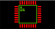
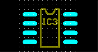
Never is there an easy way to embrace the conversion from idea to real products, but you deserve that as a creative and efficient engineer. PCBCart is able to assist you to complete this through providing high-quality and instant PCB assembly services. Our professional electrical engineers are always ready to conduct a quick yet careful check on your Gerber files and BOM so that your assembly manufacturing can be smoothly implemented with no defects or issues. When it comes to assembly confirmation items, together in accordance with PCBCart's over 20 years' experience, you should focus on aspects including spacing guidelines and fundamental requirement, part polarity, and footprint or package for assembly.
Spacing Guidelines and Fundamental Requirement
Spacing plays a critical role in determining the reliability of end products. Moreover, dimensions of our assembly equipment have to be taken into careful consideration so as to downsize failure risk of assembly. The following table details spacing guidelines and fundamental requirement, it covers leading ordinary assembly confirmation items that need to be checked by you prior to sending to us.
|
Confirmation Item
|
Subcategories
|
Specifications
|
|
Spacing
|
0402 and BGA
|
≥16mil
|
|
0201 and BGA
|
≥12mil
|
|
0603 and BGA
|
≥3mil
|
|
Component and internal shield
|
≥16mil
|
|
External edge of frame/cover and component pad (non-module design)
|
≥16mil
|
|
External pad and board edge (module design)
|
≥1.0mm
|
|
Manual soldered components and SMT components
|
>2mm
|
|
Manual soldered components and label
|
>10mm
|
|
Components mounted through adhesive and gold finger
|
Ordinarily 8mm
|
|
Components mounted through adhesive and board edge
|
Ordinarily 3mm
|
|
Between manual soldered component holes (pitch: 2mm)
|
>0.88mm
|
|
Between ICT point and component pad
|
>1.0mm
|
|
Between screw head and SMT components and soldering test points
|
>2mm
|
|
Between shielding and nearest SMT component
|
>0.3mm
|
|
Between shielding frame and nearest manual-soldered components
|
>3mm
|
|
Connector
|
Positioning holes
|
Diameter should be 0.3mm larger than that of pins
|
|
Pin-in-paste connector
|
Interference should never be acceptable.
|
|
Shield
|
Shield frame or one-piece shield
|
Thickness: ≥0.2mm
|
|
Positioning pins
|
Unsymmetrical, Quantity: 2
|
|
Hole
|
Diameter should be 0.3mm larger than that of positioning pins.
|
|
One-piece shield
|
At least 4 holes that are not regularly distributed are required.
|
|
Shield frame or one-piece shield
|
Material suggested to be copper-nickel-zinc alloy
|
|
Shield pad
|
Segmental design; width: ≥0.6mm
|
|
Transformer
|
Positioning pins
|
Diameter of holes should be 0.3mm larger than that of positioning pins.
|
|
Footprint
|
Compatible with lead
|
|
Components
|
Components with polarity
|
Should be indicated on PCB
|
|
Pin
|
Diameter of component pins should be compatible with that of PCB holes.
|
Part Polarity
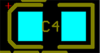
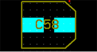
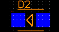
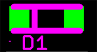
Apart from spacing guidelines and fundamental requirement, part polarity should be also designated in the silkscreen layer, which will help reduce the time taken for DFM checking of PCB assembly. Furthermore, it is better for the polarity to be visible, even after the parts have been soldered on board. The following table demonstrates some common part polarities.
|
Parts
|
Polarity Markings
|
|
Tantalum capacitor
|

|

|
|
Electrolytic capacitor
|

|

|
|
Diodes
|

|

|
|
LED
|

|

|
|
Chips
|

|

|
Footprint or Package for Assembly
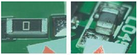
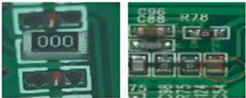
Footprint designed in the PCB file should be compatible with the part's package. This effectively means that the copper pads should be of the same size, shape and distance as those suggested in the part datasheet provided by the PCB manufacturer. Otherwise, problems such as empty soldering, cold soldering, less soldering etc. may arise, which can be shown in the following images.
• Sample Problem 1. This image indicates oversized copper pads causing components to shift after being mounted.
• Sample Problem 2. This image indicates too small copper pads eventually causing empty soldering.
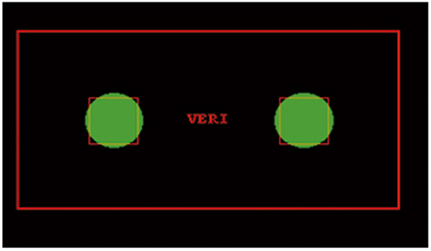
• Sample Problem 3. This image indicates that component's pin is square while copper pads are round. As such, the hole is smaller than the components' pin, making it impossible for component to be inserted into the holes.
Of course, the parameters or specifications displayed above in the table can never limit our capabilities and your design creativity. Therefore, if your design covers items beyond requirement mentioned above, just let our engineers know by leaving a note as you submit an order. We'll definitely try to meet all your design requirement.


