Active Components: This term refers to a type of component that is dependent on the flow direction of an electrical current. For example, a transistor, rectifier or valve would be considered active.
ALIVH: Short for any layer inner via hole, this is a type of technology used to build multi-layer BUM PCBs. This method uses a solder to create an electrical connection between PCB layers. ALIVH often replaces traditional vias and is a useful production method for creating high-density BUM PCBs.
Analog Circuit: It refers to circuits processing analog signals (continuous and variable signal). The output is non-binary within this type of circuit.
Annular Ring: This term refers to the copper pad area that is left after a hole is drilled through it. This ring is measured from the edge of the pad to the edge of the hole and is an important consideration in PCB design, as it allows an electrical connection to be made from one side of the hole to the other.
Anti-Solder Ball: This type of technology is commonly applied in SMT production lines with the goal of limiting the amount of tin involved in the stencil process. This is done by making a stencil on the board and creating openings at places where the solder ball tends to be produced so that the tin paste will flow to the openings.
AOI: Short for automated optical inspection, AOI refers to a type of inspection method used to find potential problems concerning soldering performance in multi-layer PCBs with components mounted on. The AOI equipment finds these issues by capturing images of the inner PCB surfaces, looking for any possible issues in terms of displacement, polarity etc.
AQL: Short for acceptance quality limit, AQL refers to the acceptable number of defective boards produced within a production run. These are identified, counted and removed during inspection. AQL is an important figure for monitoring the quality of an assembler's production practices.
Array: This word refers to the combination of multiple copies of the same PCB into a connected matrix of boards. An array may also be referred to as a panelized, stepped out or palletized PCBs. By assembling boards this way, the assembly process can be completed much more quickly. The Array # Up, in turn, refers to how many PCBs are included in the array.
Aspect Ratio: Aspect ratio refers to the ratio between a PCB's thickness and diameter of its minimum via. It's best to keep aspect ratios low to improve plating quality and minimize potential via failures.
Assembly: A process involving a series of procedures where components and accessories are placed on a PCB, resulting in a functional board.
Assembly Drawing: An assembly drawing is a reference depicting the assembly requirements of a PCB. These drawings will usually include the placements of components as well as the construction technologies, methods and parameters needed to make it happen.
Assembly House: A name used to refer to a manufacturing facility where PCBs and components are assembled. These houses will usually contain PCBA equipment such as a printer, mounter, reflow oven, and more.
Back Drilling: Primarily applied in multi-layer PCB fabrication, back-drilling helps improve signal integrity by removing stubs from plated through-holes. These stubs are unnecessary portions of via that extend into the hole, potentially causing reflections and other disturbances that damage signals.
Backplane: This is a supporting plane on a circuit board that plays an insulating role.
BGA: Short for ball grid array, this is a type of component packaging used in integrated circuits (ICs) for surface mounting. They can ensure high-speed efficiency since they use columns of balls instead of pins. BGAs are usually used to mount devices like microprocessors on PCBs permanently.
Bare Board: This term refers to a circuit board with no components mounted on it.
Blind Via: A blind via is a through-hole that connects inner layers, but it can't be seen from the exterior of the PCB.
Board: This is a shortened term for printed circuit board. This word also indicates the substrate upon which the PCB is printed. The board is an important electronic part, acting as a carrier for an electric connection between electronic components.
Board House: This is another name for the facility where PCB boards are fabricated.
Board Type (Single Unit and Panel): This indicates the manufacturing method of a PCB in terms of volume. Usually, a board is classified into one of two types: single unit or panel. In single unit manufacturing, PCBs are fabricated one by one. In panel manufacturing, on the other hand, multiple units of PCBs are manufactured in a single panel.
Body: A word used to describe the central section of an electronic component. It does not include the component's pins, leads or accessory parts.
Buried Resistance Board: The term refers to a printed circuit board with resistors buried inside. This design improves the integrity of resistant components to improve the overall function and reliability of the PCB.
Buried Via: This term is used to refer to a via connecting a top layer to one or more inner layers. In other words, a buried via can only be seen from one side of the board when looking at it from the outside.
Cable: Another word for a wire that is capable of transmitting electricity or heat.
CAD: An acronym for computer-aided design, CAD refers to a designer's use of computer and pattern equipment to develop and implement a PCB layout. The result is a three-dimensional graphic of the design, which, in this case, is the layout of a PCB.
CAE: An acronym for computer-assisted engineering that refers to schematic software packages used to develop and visualize PCB designs.
CAM Files: CAM is an acronym for computer-aided manufacturing, and the files produced by this software are used for PCB manufacturing. There are multiple types of CAM files, including Gerber files for photoplotters and NC Drill files for NC Drill machines. These files are usually sent off to board and assembly houses for refinement and eventual manufacturing.
Carbon Mask: This is a type of conductive carbon paste that is added to the surface of a pad. Made with a combination of resin and carbon toner, carbon masks are heat-cured and are typically applied to jumpers, keys, etc.
Ceramic Substrate Printed Board: This type of board is made with a ceramic substrate, to which other materials are bonded with alumina or aluminum nitride. The primary selling points for ceramic substrate boards are their excellent insulation capabilities, thermal conductivity, soft solderability and adhesive strength.
Check Plots: This is a list of check items that are based on which quality control inspection or test is implemented.
COB: Shorthand for chip-on-board, this term is a type of bare chip SMT technology. COB involves directly mounting integrated circuits to a PCB instead of packaging them first. Common in mass-produced gadgets and toys, COB can be identified by a black glob of plastic on a PCB, called a glob top. Underneath the glob, the chip connects to the board with fine wires.
Circuit: It refers to a conductive loop composed of metal leads and electronic components. It falls into one of two categories: DC circuits and AC circuits.
Coating: A coating is a solid continuous film that either protects, insulates or decorates the PCB.
Component: Alternatively called electronic components or parts, components are basic pieces that can be used to build electronic equipment and devices. Examples include resistors, capacitors, potentiometers, valves, radiators, etc.
Component Hole: This is a plated hole in a PCB that is made for a component. These holes are intended to facilitate either a component pin, termination or wire with an electric connection.
Component Library: It's a collection of components as represented in a CAD software system. It's stored in a computer data file for later use.
Component Side: This refers to the side of a PCB that contains components. The opposite side contains soldering points for components.
Connector: This term refers to a transmitting component that connects two or more active components in an assembly. Usually, connectors consist of a plug and receptacle, which can be easily joined and separated.

Copper Weight: This term is used to indicate thickness of copper foil on each layer of a PCB. It's typically expressed in ounces of copper per square foot.
Countersink Holes: These are cone-shaped holes that are drilled into a PCB. To allow a countersunk screw to sit flush with the PCB surface.
Counterbored Holes: These cylindrical holes are meant to be used with a fastener so that the fastener sits flush with the PCB surface.
Cutout: This is a groove that is dug on a PCB.
Daughter Board: The "daughter" of a "mother" board, a daughter board contains plugs, pins, sockets and connectors and plays a big role in internal connections for electronic devices and computers.
Decal: Another word for a graphic representation of an electronic component, which can also be called a footprint.
Digital Circuit: The alternative to an analog circuit. Digital circuits operate in a binary fashion like a switch, exhibiting one of two results as a consequence of an input. This is a typical circuit for computers and similar equipment.
DIP: An abbreviation for a dual in-line package, a DIP is a kind of housing for integrated circuits. This housing will typically come in the form of a molded plastic container with two rows of attachment pins.
Double-Sided PCB: A type of PCB that features traces and pads on both sides, rather than a single side.
DRC: An acronym for design rule check, this is a software verification of a PCB layout. These are often used on PCB designs before production to ensure the design doesn't contain any potential sources of error, like small drill holes or traces placed too close together.
Drill Hits: This is another way to refer to where holes will be drilled in a PCB design.
Dry Film Solder Mask: This is a type of solder mask film that is applied to a printed board that results in a higher resolution mask with finer line designs. This method tends to be more expensive than liquid solder masks.
Edge Connector: This type of connector is designed for the edge of a PCB, and it is most often used to facilitate an add-on card.
Edge Plating: This is a term used for copper plating that stretches from the top to the bottom of a surface and along the edges of a board, allowing for edge soldering and connections.
Electroconductive Paste Printed Board: This term is used to describe PCBs that are manufactured using a silkscreen printing method. The process involves applying an electroconductive printing paste to set traces and to implement stable through-hole connections.
EMC: An acronym for electromagnetic compatibility, EMC refers to the capability of a piece of equipment or system to run without producing excessive electromagnetic interference. Too much electromagnetic interference can interfere with or damage other pieces of equipment within the same electromagnetic environment.
ESD: A shorthand for electrostatic discharge, which is caused by static electricity.
External Layer: Also called an outer layer, an external layer is a layer on the outside of copper to which components attach.
Fabrication Drawing: This drawing is a way for designers to communicate a PCB design to engineers and workers. It will typically include an illustration of the board, locations and information about holes to be drilled, notes about the materials and methods involved, etc.
Fine Pitch: This term refers to a class of chip packages with micro-spacing between leads, typically below 0.050 inches.
Finger: These are metal pads found along the edge of a board. These are typically used when trying to connect two circuit boards together to expand the capacity of a computer, for example.
First Article: This is what the first manufactured board is called. First articles are usually produced in small groups before volume production begins so that designers and engineers can inspect the product for potential errors or performance problems.
FR4: This is a material rating for a flame-resistant material. It also refers to the most commonly used PCB substrate material. The name specifies that the resin material is capable of automatically extinguishing when it is aflame.
Functional Test: Alternatively called behavioral test, functional test is designed to determine how well a product's attributes meet design demands.
Gerber File: A type of CAM file used to control a photoplotter. It's a standard way of communicating board specifications with manufacturers.
Glob Top: This refers to a "glob, " a small ball of non-conductive plastic used to protect the chip and wire bonds on a COB. The glob is usually black in color and is resistant to thermal expansion, which prevents temperature changes from damaging the connection between the glob and the board.
Gold Fingers: These are connectors found on the edge of a PCB after the board has been plated with gold. Hard, smooth and flat, these fingers are excellent conductors, supporting edge-to-edge connections.
Grid: "Grid" is another term for an electrical grid, an interconnected electrical network that transmits power.

Half-Cut/Castellated Holes: This refers to holes that are drilled on the edge of a board and plated, resulting in a half-circle hole on the edge of the PCB. This is common for PCBs designed for microchip testing.
HDI: An acronym for high-density interconnector, an HDI is a type of PCB fabrication technology. It uses micro blind via technology to manufacture PCBs with high trace density.
Header: The portion of a connector assembly that mounts directly to the printed circuit.
IC: Short for integrated circuit, an IC is also called microcircuit, microchip or chip. Essentially, IC describes a method for miniaturizing circuits, especially for semiconductor devices.
Internal Layer: This term refers to the inner layers in multi-layer PCBs. These inner layers are mostly signal layers.
IPC: An abbreviation of Institute of Printed Circuits, a worldwide non-profit association dedicated to the design of PCB wiring. The group helps enterprises achieve greater business success by helping them meet rigorous manufacturing standards, which, in turn, improve overall quality standards.
Kapton tape: Alternatively called polyimide tape, this electrically insulating tape has numerous useful features, including heat resistance, inextensibility and thinness.
Laminate: This term refers to the combination of different materials through heating, adhesive and welding methods to create a new material with multiple layers. The resulting material has greater strength and stability than the individual materials combined to create the laminate.
Laser Photoplotter: Alternatively called a laser plotter, this type of photoplotter creates a finely-lined raster image of the end product. The result is a high-quality, highly accurate plot.
Layer-to-Layer Spacing: This is the distance between PCB layers. The lower the spacing, the more difficult the manufacturing process will be.
Lead: Another word for a terminal on a component.
Legend: This is a shorthand guide for marking component names and positions. Legends help ease the assembly and maintenance processes.
LPI: Shorthand for Liquid Photoimageable, an LPI is a liquid solder mask that is sprayed on a PCB. This method is more accurate, thinner than a dry film solder mask and more affordable.
Mark: A term used to refer to a set of patterns for optical localization. Marks can be classified into PCB Marks and local Marks.
Membrane Switch: A membrane switch is applied to the front of a finished PCB. It indicates functions of the PCB and components, such as key functions, indicators and other parts. The membrane also provides protection for the PCB in the form of waterproofing and humidity protection.
Metal Base/Core Printed Board: Metal core PCB refers to a type of PCB with a core material made of metal instead of plastic, resin or FR4 material.
Mil: A "mil" is another way to say a thousandth of an inch. It's also the equivalent of a "thou. "
mm: "mm" is another way to express a millimeter or a thousandth of a meter.

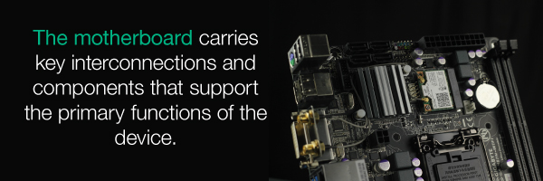
Motherboard: This is the main board in a computer or electric device. The motherboard carries key interconnections and components that support the primary functions of the device.
Mounting Hole: This hole is intended to secure the PCB to its final location in a device. To ensure there is no interference, all mounting holes are non-conductive and unplated.
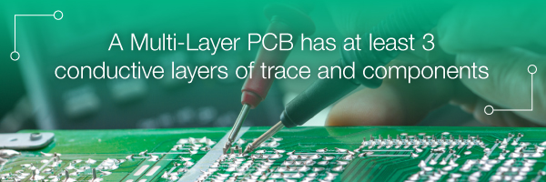
Multi-Layer PCB: This is a type of PCB with at least three conductive layers of trace and components.

Multimeter: A testing tool used to measure electrical values like current, resistance and voltage.
Multi-Wiring Printed Board: An equivalent to a multi-layer printed circuit board, this term refers to PCBs with multiple layers of trace, with dielectric layers between each.
NC Drill: This is a more common name for a Numeric Control drill machine. This type of machine is what assemblers use to drill holes in PCBs.
Node: This is a pin or lead that is connected to at least one wire.
NPTH: An acronym for non-plated through hole, NPTH refers to a hole with no plated copper on the hole wall. This means no electric connections can be made using the walls of this hole.
Open: This is a short way of saying "open circuit, " which is a break in an electrical circuit's continuity. This prevents current from flowing and can disrupt the proper function of a PCB.
Pad: This is one of the most basic composition units of a PCB assembly. A pad is a contact point used to connect components with a via and is the point to which the components are soldered.
Panel: A panel is a combination of boards produced simultaneously to improve efficiency during the manufacturing process. Once the process is finished, these panels are typically broken apart into their singular units before being used.
Panelize: This is the act of grouping multiple PCBs into a panel to improve manufacturing efficiency. An alternative term is panelization.
Part Number: This is an identification method used in industry to differentiate parts from one another. It's also used to identify specific parts, which is helpful in identifying problematic assembly batches and preventing incorrect product applications.
Part: This is another word for a component, or a basic piece of electric equipment, such as a resistor, capacitor, potentiometer, valve, radiator, etc.

PCB Base Material: The material upon which the PCB is built. The PCB base material is typically composed of resin, metal, ceramic or another material with thermal and electric properties that support the PCB's final function.
PCB Database: All the data that is or could be used for a PCB design. This data is usually stored in a computer file.

PCB: An abbreviation of Printed Circuit Board, a PCB is a board that contains a conductive material and components, which act in synchrony to produce a designed response. PCBs rely on electrical circuits, which are either printed or soldered onto the board to elicit the desired result. Printed circuit boards are available in a wide variety of shapes, sizes and purposes to suit any industry or application.
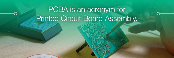
PCBA: This is an acronym for Printed Circuit Board Assembly, where a company solders components to boards.

Peelable Solder Mask: A solder mask or layer of solder mask that can be peeled from the board.
Photoplotter: A device used in manufacturing to produce artwork onto film by plotting objects instead of images.
Pick-And-Place: A method of SMT assembly where a machine automatically picks up SMDs and places them in the correct positions on the board.
Pin: A terminal on a component. It is also called a lead.
Pitch: The distance between pin centers of SMDs.
Plated-Through Hole: Alternatively called a PTH, this is a procedure in which a through-hole is plated so that the hole wall can be conductive. This is often used as a contact point for through-hole components and can be used as a via.
Prepreg: Also called PP, is the key material for multi-layer PCB manufacturing. it is primarily composed of resin and strengthening material that is then classified into glass-fiber cloth, paper base, compound material etc.
Press Fit Holes: This is a hole through which a contact terminal can be pressed into a PCB.
Printed Wiring: A process where a design is etched into conductive metal on a board, producing a wire design for the PCB.
Printing: Part of the PCB manufacturing process where a circuit pattern is printed on the board.
PWB: An acronym for Printed Wiring Board, which is another name for a PCB.
Reference Designator: Alternatively called "Ref Des, " this is the name of a component on a PCB. Typically, the component name begins with a letter or two, indicating the component class, followed by a number. These designators are usually printed on the silkscreen to help identify each component.
Reflow: This is the process of melting solder to create a joint between a pad and a component or lead.
RF: Short for radio frequency, RF is an electromagnetic frequency ranging between 300KHz and 300GHz. RF can also be a type of high-frequency electromagnetic signal.
RoHS: Alternatively known as the Restriction of Hazardous Substances, RoHS is a European environmental protection law. Many global companies must follow RoHS standards to sell products in the EU.
Route/Track: This is the layout of a PCB's wiring structure, which is important for the proper function of the PCB. As a verb, the act of routing means designing such wiring structures.
Schematic: A technical drawing that illustrates the connections between PCB components. Schematics will often include abstract representations of components instead of pictures and is an important first step in PCB design.
Short: This is an alternative way to say "short circuit, " which is a connection with low resistance, resulting in excess current at the connecting point. This can cause serious problems in the PCB, including failure.
Silkscreen: This is a layer of epoxy ink applied to a PCB that contains component names and positions. The labels included on silkscreens help to direct workers through the assembly process. Typically, silkscreens are white, which helps the labels stand out against the PCB's solder mask.
Single-Sided PCB: A PCB design with traces and pads included on only one side of the board.
Slot Hole: Non-round holes on a PCB that may or may not be plated. These are often required for specific components but are costly due to the labor needed to cut them.
SMD: Short for surface mount devices, it refers to components designed to be soldered on the surface of PCBs, rather than through a thru-hole.
SMT: Short for surface mount technology, this type of assembly technology directly solders SMDs to the surface of a PCB, rather than running components through thru-holes. This allows the board to function without drilling holes through it and also helps improve component density on the surface of the PCB.

Solder Mask/Solder Resist: This is a layer of material, usually consisting of an epoxy resin, which isn't compatible with solder. This material is applied to the entire PCB, except those areas where content needs to be soldered. This process helps to physically and electrically insulate traces, preventing shorts. Solder masks are often green in color, though red and black are also common.
Solder Side: This is the opposite of the component side and is usually regarded as the bottom side.
Spacing: This term refers to the distance between wires on a PCB.
Substrate: This is another word for "PCB base material", the primary material for PCB fabrication. Generally, this material can be flexible or rigid and can be made of epoxy, metal, ceramic or other materials. The function of the end PCB will usually determine which substrate will be used for the project.
Supported Hole: This is a via with pads on both sides of the PCB. It's also plated inside the via. This means the entire hole can support functions relating to thermal or electrical conductivity.
Surface Finish: Since copper tends to oxidize in natural environments, a surface finish protects the layer from doing so. Oxidation can cause the tin paste to fail or solder incorrectly. The primary types of surface finishes include HASL, ENIG, IMAG, OSP and others.
Tented Via: This is a type of via that has a dry film solder mask covering both its pad and its plated-thru hole. This solder mask insulates the via completely, protecting the PCB against shorts. Some vias are tented only on one side to allow for testing on the other.
Thou: This is shorthand for a thousandth of an inch. It's another way to say "mil. "
Through-Hole/Thru-Hole: This refers to a hole passing through at least two layers of a multi-layer PCB. It's also used as a descriptor for components with parts or pins that run through a board to be soldered to another side.
Trace/Track: This refers to the copper path printed on a PCB. It functions similarly to an electrical wire, connecting components on a PCB board. The word "trace" is also used to refer to a segment of the path.
Tracing: This term refers to the width of a PCB's wires.
UL: UL stands for Underwriter's Laboratories, Inc., a renowned company specializing in establishing safety standards and independently assessing products according to these standards.
Unsupported Hole: This type of hole has a pad on the solder side, but no pad on the component side. There is also no metal layer inside the hole. This means the hole has no conductive reinforcement.
Vector Photoplotter: Alternatively called a vector plotter or Gerber Photoplotter, this type of photoplotter draws a plot line by line using light manipulation technology. This method can produce larger plots, but it is also much slower than the more modern laser photoplotter method.
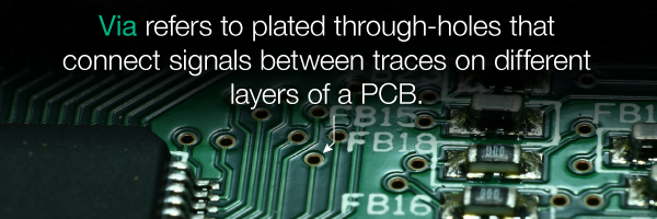
Via: This term refers to plated through-holes that connect signals between traces on different layers of a PCB. These holes have conductive copper interiors to maintain an electrical connection.
Via Filled With Resin/Via Plugged: This is a via that is filled with an epoxy resin. Once filled, copper can be soldered to the surface of the resin without influencing the final product.
Via in Pad: Also called a thru-hole on the pad, a via in pad functions as an electric connection between layers. It is useful for multi-layer components or for fixing the positions of components.

V-Scoring: This is an incomplete cut through a panel, which is often used to help break apart panels of PCBs into single units.
Wire: This refers to a conductive cable that can transmit electricity or heat. It also refers to a route or track on a printed circuit board.
PCB terminology consists of a technical group of acronyms and terminologies essential in the printed circuit board industry. They define the various testing, inspection, and evaluation processes associated with PCB design, production, and quality assurance.
Understanding these terms, along with the corresponding abbreviations and standards, is important during the design, production, and testing stage of PCB manufacturing. Being a professional PCB manufacturer, PCBCart has rich experience and technical expertise in providing high-quality PCB solutions and services. PCBCart is committed to providing customized PCB design, production, and testing services to customers to satisfy industry standards and customer needs.
Get an Instant Quote for PCB Assembly & PCB Manufacturing
Helpful Resources
• PCBCart's Advantages over other PCB Manufacturers - Why should you chose PCBCart?
• Standard PCB Fabrication Service with Multiple value-added Options
• Quickturn PCB Prototyping Service
• Aluminum PCB Fabrication Service
• Flexible PCB Fabrication Service
• Flex-rigid PCB Fabrication Service
• High Frequency PCB Fabrication Service
• Thick Copper PCB Fabrication Service
• High -Tg PCB Fabrication Service
• Halogen-Free PCB Fabrication Service
