


PCB successfully added to your shopping cart
Layer Stackup
The irreversible development of modern electronics has been increasingly pushing PCBs towards such demands as miniaturization, light weight, high speed, better functionality and reliability, and longer lifetime, which results in the popularity of multilayer PCBs. Combined by a type of semi-solid adhesive which is called "prepreg", two or more single and/or double-sided PCBs are stacked together to generate multilayer PCBs through reliable predefined mutual connection between them. There are three or more conductive layers in one multilayer PCB with two layers outside and one layer synthesized in the insulation board. With the increase of PCB complexities and densities, it's possible for some issues to take place such as noise, stray capacitance and cross talk when layer arrangement gets inefficient design.
Planning optimal multilayer stack-up is one of the most important elements in determining the Electromagnetic Compatibility (EMC) performance of a product. A well-designed layer stack-up can both minimize the radiation and can stop circuit from being interfered by external noise sources. Well-stacked PCB substrates can also reduce signal cross talk and impedance mismatch issues. However, an inferior stack-up may get EMI (Electromagnetic Interference) radiation rising, because reflections and ringing in the system as a result of impedance mismatch can dramatically lower products' performance and reliability. This article then focuses on layer stack up definition, its designing rules and essential considerations.
What is Stack-up?
Stack-up refers to the arrangement of copper layers and insulating layers that make up a PCB prior to board layout design. While a layer stack-up allows you to get more circuitry on a single board through the various PCB board layers, the structure of PCB stackup design confers many other advantages:
• A PCB layer stack can help you minimize your circuit's vulnerability to external noise as well as minimize radiation and reduce impedance and crosstalk concerns on high-speed PCB layouts.
• A good layer PCB stack-up can also help you balance your need for low-cost, efficient manufacturing methods with concerns about signal integrity issues
• The right PCB layer stack can enhance the Electromagnetic Compatibility of your design as well.
It will very often be to your benefit to pursue a stacked PCB configuration for your printed circuit board-based applications.
For multilayer PCBs, general layers include ground plane (GND plane), power plane (PWR plane), and inner signal layers. Here's a sample of an 8-layer PCB stackup.

PCB Layer Stackup - PCBCart
In accordance with this figure, it's obviously clear to indicate layer distribution in PCBs conforms to a symmetrical or balanced structure. Apart from layer distribution, the spacing between layers should be taken seriously as well. To meet the requirement of miniaturization, minimum trace spacing must be obtained while planning layer stack-up. The space between layers can be either core or prepreg. Multilayer boards usually consist of at least one or more cores and prepregs. Cores are made up of a copper-plated glass-reinforced epoxy laminate sheets. The thickness of core is in the range from 0.1mm to 0.3mm.
Prepreg is the common term for a reinforcing fabric which has been pre-impregnated with a resin system. This resin system (typically epoxy) already includes the proper curing agent. The main function of prepreg is to stack all layers into a whole board by high temperature. The following table shows physical and chemical attributes of main categories of Prepreg, that is, 7628, 2116 and 1080.
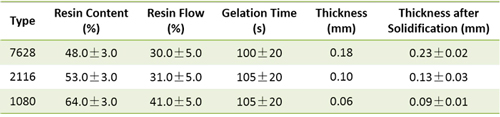
Actually, thickness of each type of prepreg isn't always stable and adjustments will be made to meet specific PCB thickness demand. Some factors have to be taken into consideration when determining the count of prepreg including thickness of inner layer, product design thickness requirement or manufacturing technology requirement, features of prepreg, practical performance and the actual thickness after stack-up trial. Below image indicates a sample 4-layer PCB whose layer distribution and thickness are depicted.

In this example, as copper thickness is stable, PCB maker will adjust thickness of prepreg and core to meet thickness need. There're 2 methods to be compatible with the adjustment mentioned above.
• Interlayer offset. Resin recession groove is used in board side design instead of choked flow pad. In regards with stack-up positioning, hot melting plus rivet plus dowel method can be used to solve stack-up offset problem.
• Stack-up measling. In the process of board arrangement, silicon pads can be added, together with the assistance of epoxy plate so that pressure will remain balanced, which can both help eliminating stack-up measles and effectively control the uniformity of board thickness.
Based on chemical and physical attributes of prepreg, you have access to estimate thickness or copper weight of final circuit board through an easy calculation.
To obtain specific thickness of prepreg, different types of prepregshave to be combined together to achieve required thickness. For example, the thickness of 0.14mm derives from combination of two sheets of 1080 prepregs while that of 0.19mm from combination of 2116 and 1080 prepregs.
PCBCart's Standard PCB Layer Stack-up
PCBCart provides multilayer circuit boards with layers in the range from 4 to 32 layers, board thickness from 0.4mm to 3.2mm, copper thickness from 18μm to 210μm (0.5oz to 6oz), inner layer copper thickness from 18μm to 70μm (0.5oz to 2oz), and minimal spacing between layers to 3mil.
Following images present PCBCart's commonly used stack-up for Standard PCB service. The actual layer stack-up will be determined by PCB material and many other elements. If you have special requirements on PCB layer stackup, please send your circuit board thickness and layer count by email. We'll share corresponding stack-up accordingly.
Note: Our PCB Prototype Service offers limited possibilities on custom layer stackup. If your application asks for specific layer stack-up, we recommend Standard PCB Service.
A commonly-used Layer Stackup for 4-layer PCBs

A commonly-used Layer Stackup for 6-layer PCBs

A commonly-used Layer Stackup for 8-layer PCBs

A commonly-used Layer Stackup for 10-layer PCBs

A commonly-used Layer Stackup for 12-layer PCBs

Choose PCBCart for Your PCB Layer Stack-Up Needs
If you like the idea of PCB stack-up for your electronic applications, the BEST place you need to go for layer stack up is PCBCart. We offers full-service turnkey solution for all things concerning PCBs. We can help you with:
• Develop your layer stackup in PCB design
• Fabricate your stack PCBs
• Create prototypes to test your designs for any possible flaws
• Do full PCB runs
With over twenty years of experience in the area of printed circuit boards manufacturing, you are sure that PCBCart is a name you can rely on for your multi-layer PCBs and all your PCB-related needs. We excel at speed of order turnaround, quality and value to an extent that other fabricators of printed circuit boards cannot match. Our standard PCBs meet the stringent IPC2 standard of quality, and our company is fully ISO9001:2008 compliant. Prefer discussing with us about your PCB layer stackup demands? Reach us here. Or click the button below to get an online PCB quote
Quote for PCB Fabrication With Custom Layer Stackup
Helpful Resources
• PCB Composition and Its Material Selection Guide
• Factors Determining the Number of Layers and Layer Distribution in PCBs
• Multilayer PCB Benefits and Applications
• PCBCart Offers Custom Layer Stackup based on Your Custom Demands. Get PCB Quote Now!