
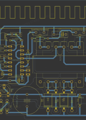
PCB Layout Design
As a company that has served the global electronics industry for more than 20 years, PCBCart provides a one-stop electronic manufacturing service that starts with the PCB layout.
Start Your Layout Quote

 English
English
English
English
English
 Español
 Deutsch
 Français
 Italiano
 日本語
日本語
 ภาษาไทย
 Malay
Malay
PCB Layout Design
As a company that has served the global electronics industry for more than 20 years, PCBCart provides a one-stop electronic manufacturing service that starts with the PCB layout.
Start Your Layout Quote
PCB Layout Capabilities
| Maximum number of layers |
64 |
| Maximum number of pins |
150,000+ |
| Maximum number of connections |
120+ |
| Minimum line width |
3mil |
| Minimum line spacing |
3mil |
| Minimum via hole |
6mil (4mil for micro via do with laser) |
| Maximum number of BGAs |
120+ |
| Minimum BGA pitch |
0.3mm |
| Maximum number of BGA pins |
18865 |
| Maximum Speed Signal |
224G-PAM4 |
Chip and Module Solutions for Advanced PCB Layout
From Data Centers to Automotive Systems: Master Multi-Industry Processor, FPGA, Power, and Memory Design Strategies.
Data Center/Server Processors
Networking/Communication Processors
Industrial Control Processors
Mobile/Embedded Processors
Automotive Processors
High-Performance Computing FPGAs
Military/Industrial-Grade FPGAs
Low-Power Embedded FPGAs
Multi-Channel Power Management ICs (PMICs)
Automotive-Grade Power Chips
High-Density DC-DC Converters
High-Speed Network Interfaces
High-Speed Serial Interfaces
Data Converters (ADC/DAC)
High-Performance DRAM
Industrial-Grade Storage
Low-Power Memory
Autonomous Driving Domain Controllers
Vehicle Body Control & Safety
Smart Cockpit Domain Controllers
PCB Layout Design Process
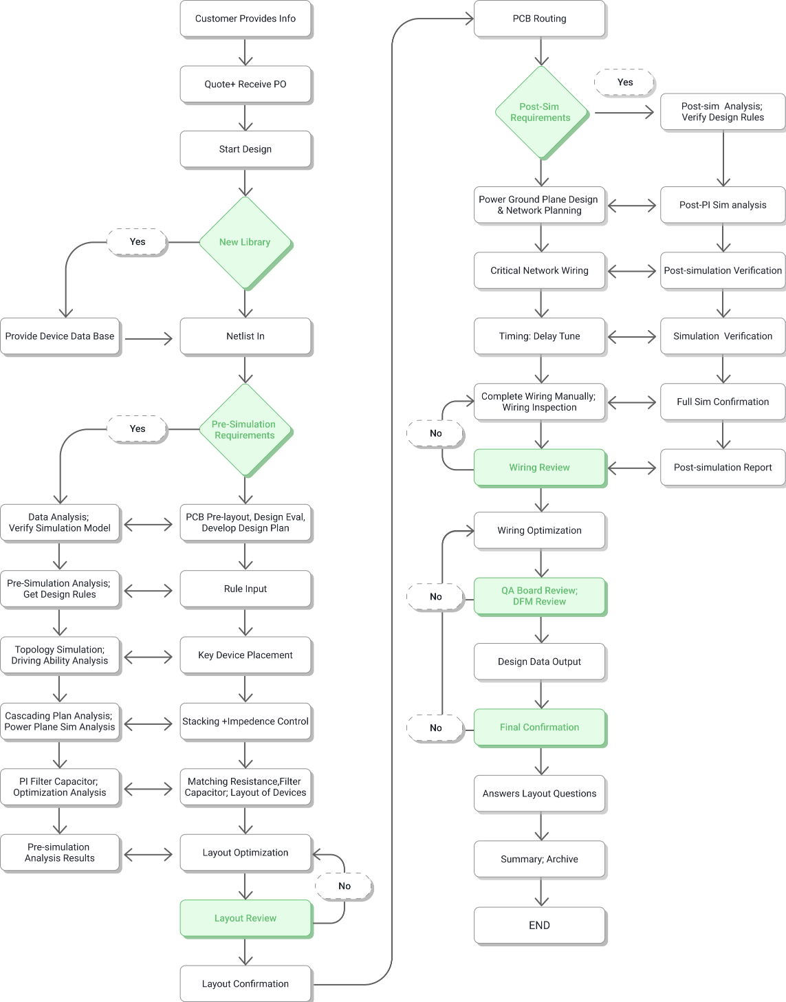
Layout Work Flow at PCBCart


PCB Layout Design Cycle

| PCB board PIN number | Lead Time (working days) |
|---|---|
| 1-1000 PIN | 3-5 days |
| 2000-3000 PIN | 3-8 days |
| 4000-5000 PIN | 8-12 days |
| 6000-7000 PIN | 12-15 days |
| 8000-9000 PIN | 15-18 days |
| 10000-12000 PIN | 18-20 days |
| 13000-15000 PIH | 20-23 days |
| 16000-19000 PIN | 23-30 days |
Note: The design cycle of the above PCB board PIN number is the regular delivery period. The accurate design cycle is based on the time when the customer provides complete information and the difficulty of the PCB board for comprehensive evaluation.
Advantages of PCB Layout Service at PCBCart

Prolific + Professional Engineers
Significant Seniority: More than 20 years of Industry Experience. Efficient Design: Ordinary PCB layouts can be completed in minutes.
Excellence in Quality
Self-inspection: Detailed checks on design aspects using a checklist. Expert Review: Senior experts assess design, manufacturability, testability, EMC, and thermal factors.
Quick-Turn Assembly Services
Parallel Design: Reduces delivery time by 30-50%. In-House Production: Enables immediate manufacturing.
Expert & Secure Layout Solutions
Software Compatibility: Proficient in Altium, PADs, OrCAD, EAGLE, and KiCAD. NDA Protection: Mandatory NDAs to safeguard customer innovations.
One Board Success
Right the First Time: Streamlining PCB development, reducing R&D iterations. Rapid Market Entry: Seizing the First-Mover Advantage.
Cost Optimization
Manufacturing Compatibility: Increased supplier flexibility, and reduced supply chain risk. Optimized for Scale: Design considerations for R&D and manufacturing.Quality Assurance
We ensure excellence through self-checks, mutual inspections, expert reviews, and stringent standards.


Expert Guidance
Comprehensive 'Design Guidelines' and 'Design Specifications' offer additional technical recommendations beyond layout.
Self-Inspection
Comprehensive checks across all design facets (layout, wiring, thermal, etc.) using detailed checklists and strict quality systems.
Mutual Inspection
Standardized peer reviews and thorough Design for Manufacturability (DFM) analysis.
Expert Review
Final review by senior engineers, encompassing design principles, DFM, Design for Testability (DFT), Signal Integrity (SI), Power Integrity (PI), and Electromagnetic Compatibility (EMC).Industry Involved

Telecommunications
Switches, routers, 4G/5G equipment, network transmission, optical networks.

Medical Technology
Ultrasound, MRI, CT, IVD, temperature measurement, blood analysis, digital X-ray.

Computing
Servers, laptops, storage, tablets, cloud computing.

Industrial Automation
AI, machine vision, smart manufacturing, smart grids, clean energy, machinery, and fire safety.

Semiconductor
Integrated circuits, consumer electronics, communication systems, photovoltaics, power conversion.

Rail Transportation
Transit vehicles, electromechanical systems, autonomous operations, and dispatch systems.

Consumer Electronics
Smartphones, cameras, wearables, VR, IoT devices.

Electric Vehicles
Powertrain, chassis, autonomous driving, intelligent systems, and electronic systems.
 [email protected] [email protected]


