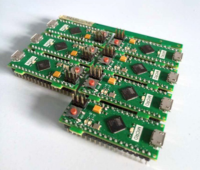
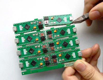
Panelization is a must-have with the consideration of PCB manufacturing efficiency. On the one hand, panelization leads to the improvement of PCB manufacturing efficiency so that lead time can be reduced. On the other hand, for small PCBs with irregular shapes, panelization is the most effective manufacturing way. For PCB assembly, panelization is helpful because it can downsize the cost of labor and it's convenient to control products'quality.

However, panelization has some restrictions as well. The size of whole PCB panel must conform to the manufacturing capabilities of automation equipment including paste printers, SPI equipment, SMT machines, reflow oven, AOI equipment, AI Panasert and wave-solder machines. Generally speaking, the maximum size of overall layout is 450x330mm while the minimum size of overall layout is 50x50mm. Some irregular PCBs that have small sizes and can't be panelized only rely on auxiliary vehicle for assistant fabrication.
However, a problem always remains prominent in the process of panelization when PCB manufacturers and SMT fabricators fail to take full consideration of manufacturability and to reach the benefit maximization of manufacturing cost. They have to depend on the most suitable combination methods according to specific PCB requirement with consideration of cost and manufacturing capability.
Some combination methods of panelization are displayed as the follows:
• Order Panelization
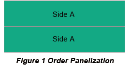
As a common method, order panelization is the most massively-used panelization method. Lots of advantages contribute to its present leader status. Firstly, this type of panelization is compatible with all circumstances, with no considerations to be taken of SMT manufacturers fabrication conditions and product combination. Secondly, order panelization isn't influenced by manufacturing number, allowing the maximum number of panels effectively based on the maximum number of SMT equipment so that it leads to highest manufacturability among all combinations of panelization. Thirdly, printing quality won't be decreased due to the influence of pad orientation of special components in the process of printing stencil design. Finally, operating difficulty won't be accumulated owing to the different orientations of panels in each run of the whole procedure.
For PCB manufacturers, the cost is acceptable as well with the method of order panelization and quality can be maintained at the highest level. Order panelization can be displayed in Figure 1 below.

• Rotation Angle Panelization
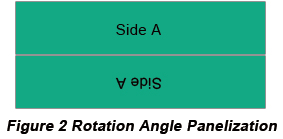
In order to reach the optimal utilization of board materials and decrease the waste of board materials, panelization is implemented by rotating 90 or 180 degrees, which is called rotation angle panelization. This type of panelization caters to disabilities of order panelization as a result of the space vacancy by special components.
Rotation angle panelization features some disadvantages. Firstly, mounting efficiency is possibly decreased after angle rotation. And mounting quality will possibly stay away from stable state. Operating strength of workers will also be increased in terms of visual inspection after assembly since each time has to see a direction change, leading to high probability of mistakes. Rotation angle panelization displayed in Figure 2.

• Double-side Panelization
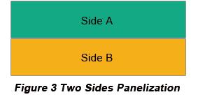
Displayed in Figure 3, double-side panelization refers to panelization in which both sides of a PCB are panelized on one side as a panel.

This type of panelization is available for PCBs of which both sides have no big-volume and poor heat resistivity components. Otherwise, components on the back side of a PCB with high volume and weight will possibly fall off and components with poor heat resistivity will be burned.
This type of panelization features some advantages. Firstly, it does well in increasing SMT overall efficiency and decreasing manufacturing cost. Double-layer PCB fabrication can be completed through one-time craft, saving a printed stencil and time spent on products switch and greatly increasing the utilization efficiency of SMT equipment. Secondly, only one curve of specimen is required in accordance with reflow soldering and wave soldering so that material of curve of specimen can be saved. Furthermore, the management strength to field manufacturing won't cause too much waste so that this type of panelization is suitable for mass production.
This type of panelization features disadvantages as well. Firstly, PCBs with BGA are not suitable for this type of panelization since it'll lead to difficulties to rework. Secondly, the quantity of manufacturing products suffers from limitations because panels must be arranged based on even numbers. Otherwise, scrap of a board will be generated. Thirdly, AI and DIP can't be carried out until cutting is finished so that plug-in efficiency and DIP utilization rate will be influenced. Finally, more difficulties will be exposed to substrate manufacturers in that it's difficult for them to control quality.
• Combination Panelization
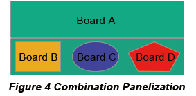
Combination panelization, also called characteristic panelization, is a type of panelization in which different types of PCBs are combined together according to combination principles. It is displayed in Figure 4 below.

This type of panelization features some advantages. Firstly, it is suitable for the manufacturing model containing multiple PCB combinations in products like household appliances and toys. Secondly, it is beneficial to production efficiency improvement and cost shrinking so that products turnover and semi-finished products stock can be greatly reduced, which is capable of meeting customers' requirement of fast shipment.
However, this type of panelization features disadvantages as well. On one hand, in the process of assembly line work, products differentiation is difficult to manage, leading to product chaos. On the other hand, when one board among the combination suffers bad quality or even scrap, the overall number of panelizations will go down and it's bad for manufacturing remediation.

The ideal combination ways of PCB panels are determined by manufacturing efficiency, difficulty and cost and depanelizing methods are extremely significant and essential, with the most commonly-used methods of V-groove and snap hole. In the process of depanelizing method design, pressure must be taken into full account in order to obviate the deformation caused by reflow and ensure the convenience of depanelization. Snap holes are mostly utilized for PCBs whose thickness is 1.0mm below and have external force-sensitive components such as BGA so that possibilities of reflow deformation can be reduced to ensure quality, improve the manufacturing efficiency and distribute external force.
PCBCart Offers Free PCB Panelization!
As a value-added option of our custom PCB manufacturing service, we offer FREE PCB Panelization service. You are welcome to send the PCB design file of single unit, we will do the file panelization work and produce your boards in panel types! You will only be charged for the PCB fabrication cost. Isn't this fascinating? If you have the PCB Gerber file in hands, feel free to click below buttons to get your PCB fabrication costs within seconds, or you may simply reach us here for further information and manual quotation.
Quote for FR4 PCBs Fabrication Online
Helpful Resources
• What is PCB Panelization And How It Helps with PCB Assembly and Fabrication
• Full Feature PCB Manufacturing Service from PCBCart - Multiple Value-added options
• Advanced PCB Assembly Service from PCBCart - Start from 1 piece
• How to Order PCB as Panels with PCBCart
