
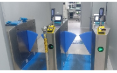
BGA Assembly
High-Precision BGA Assembly for AI, 5G and More
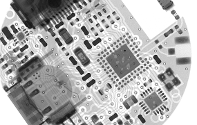
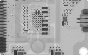
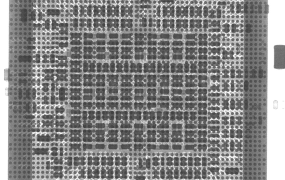
 Ultra-Fine 0.35mm Pitch
High First-Pass Yield Rate
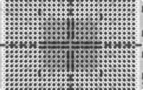
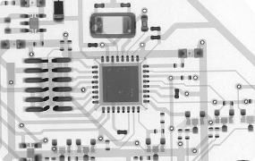
100% X-ray Inspection

 English
English
English
English
English
 Español
 Deutsch
 Français
 Italiano
 日本語
日本語
 ภาษาไทย
 Malay
Malay
BGA Assembly
High-Precision BGA Assembly for AI, 5G and More
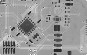
Ultra-Fine 0.35mm Pitch
High First-Pass Yield Rate
100% X-ray Inspection
BGA Assembly Capabilities

| Capability | Standard |
|---|---|
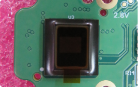
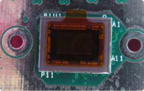
| Types of BGA |
- Plastic Laminate BGA (PBGA) - Tape Ball Grid Array(TBGA) - Ceramic Ball Grid Array (CBGA) - Flip Chip Ball Grid Array (FCBGA) - Enhanced Ball Grid Array (EBGA) - Micro BGA - Package on Package (PoP) - Chip Scale Package (CSP) - Wafer level chip scale packaging (WLCSP) |
| BGA CSP |
Package Dimension: from 5mm x 5mm to 45mm x 45mm Minimum Solder Ball Pitch: 0.3 mm/0.5 mm Minimum Solder Ball Diameter: 0.15 mm/0.25 mm Minimum Solder Ball Height: 0.25mm |
| Chip Package |
BGA/LGA/HDA/POP/uBGA/WLCSP/CSP |
| Quality Assurance |
- Automated Optical Inspection - X-ray inspection - Functional Testing |
| BGA rework |
- PCB Reballing - BGA Site Modification - Correcting Damaged or Missing BGA Pads - Component removal and replacement |
BGA Product Assembly Process at PCBCart
At PCBCart, our process for assembling BGA (Ball Grid Array) components is all about precision and quality. From the moment materials arrive, every phase—initial material inspection, precision soldering, meticulous testing, and secure packaging—follows industry standards and meets our clients' needs. Our experienced technicians use advanced technology and skilled techniques, with strong quality checks throughout, to create high-performance and reliable BGA products. Trust PCBCart to turn your designs into strong and dependable solutions, ensuring every detail is perfect.
Key Points & Control in BGA Product Production
| Process | Key Points | Control Method | Picture |
|---|---|---|---|
| PCB Design |
1. Pad design 2. Residualcopper rate 3. High Tg board 4. Layout method 5. Surface finish 6. Lead or lead free |
1. Reference IPC Specification 2. Specification of parts 3. Gerber file Review 4. DFM check (30mm from the edge of the board) 5. Pad size: BGA pad 08~1.2 6. Pad type: NSMD 7. Layout, stamp holes design 8. Residual copper rates≤15% |

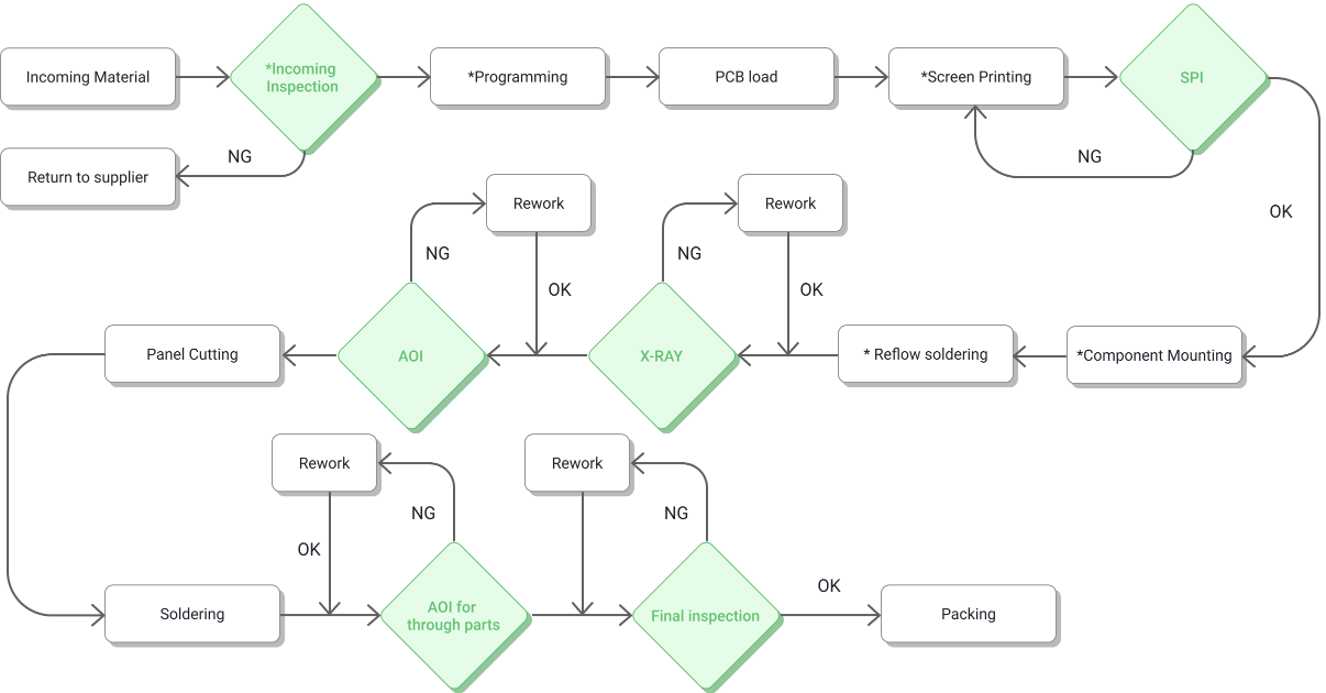
NON Solder Mask Defined 
Solder Mask Defined (Not Recommended) |
| Producibility Review |
1. Whether the pad design is reasonable 2. Whether the parts interfere 3. Confirm the layout 4. Confirm the BOM 5. Confirm the pick and place file 6. Confirm the special process |
1. DFM software&PCB design specification 2. Output DFM reports and suggestions 3. Suggest the layout 4. Polarity confirmation 5. System control 6. List of ESD sensitive components 7. Temperature specification list of parts |

DFM checking softwarer 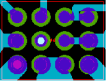
unreasonable design Via is unfilled and plated in the pad |
| PCB Fabrication |
1. Confirm PCB specifications 2. PCB manufacturing capability 3. Define PCB process & parameters 4. Production data documents 5. Test &packaging protection |
1. DFM software 2. Output the DFM report and propose EQ 3. Communicate with customer&Confirm abnormity 4. Make manufacturing order 5. CAM data production 6. PCB fabrication 7. QC,FQC, AOI 8. Test and final inspection 9. Packing |
A = Via pad on package B = Land pad on PCB |
| Incoming Material & Storage |
1. Quantities & Batches 2. Packaging 3. Quality inspection 4. Storage conditions 5. Chip material wear |
1. Bar code & System control 2. Bake & vacuum pack 3. Defective DMR 4. Oven parameters 5. Bake records 6. Feeding confirmation record 7. ESD control |

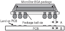
Bake 
Vacuum package |
| Stencil & Jigs |
1. Thickness of stencil 2. Opening mode of stencil 3. Ratio of width to thickness 4. Stencil production process 5. SMT jigs |
1. Confirm the final opening stencil file 2. Stencil opening specification 3. Tension confirmation 4. Hole wall observation 5. System logging 6. IPC-7521 specification |
Stencil confirmation |
| Production Arrangements |
1. Confirm BOM &SOP 2. Confirm the moisture sensitive components 3. Confirm whether the PCB is baked 4. Key material packing method 5. ESD protection & temperature and humidity control 6. Production requirements 7. Material accuracy |
1. MES process control & online SOP 2. Electrostatic grounding,electrostatic bracelet 3. Special process mark 4. Baking system record 5. Feeding list & temperature and humidity spot check list 6. List of quantities 7. Key control propaganda |
ESD electrostatic gate 
Personnel ESD electrostatic protection |
| Printing |
1. Parameter of printing 2. PCB flow direction 3. Solder paste selection 4. Solder paste back temperature 5. Stability of equipment 6. 5S |
1. SPI monitoring 2. Support fixture use 3. Printing parameter confirmation 4. Solder paste MES control 5. Process system control 6. First article confirmation 7. PCB lot &Package &Quantity 8. Substrate box transportation |

100% SPI 
3D imaging of solder |
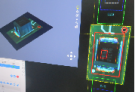
| Parts Mounting |
1. Mounting parameter 2. Program version 3. ESD & Temperature and humidity 4. Correct material 5. Nozzle use 6. Transfer board 7. Time management |
1. Feeding list (Nozzle,Feeder) 2. Quality&Production check materials 3. Spot check of equipment 4. Transmission board speed setting 5. X-ray confirmation 6. Electrostatic ring,electrostatic glove,ion air gun 7. First article confirmation of the three parties (production,engineering, quality) 8. MES control 9. SOP&5S control 10. Solder paste board production time≤2H |

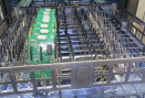
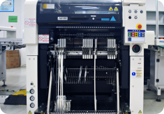
High precision mounting machine 
X-ray inspection machine 
First article confirmation |
| Soldering (reflow + selective soldering) |
1. Furnace temperature parameters 2. Oxygen content ≤7000PPM 3. Temperature measurement plate&furnace temperature curve 4. Equipment temperature zone ≥10, nitrogen 5. The welding appearance conforms to IPC Class iii 6. Bubble ≤25% 7. Climb tin height ≥75% 8. Choose to weld the through parts 9. ESD&Temperature&Humidity control |
1. Temperature measuring plate (BGA solder joint position) 2. Uniform distribution of temperature measurement points 3. Measured furnace temperature curve 4. Oxygen content real-time monitoring 5. Printing to reflow soldering time(single side ≤4H,double side s12H) 6. Set the maximum temperature based on the specification 7. Board direction 8. The smooth conveyor belt 9. Solder paste specification 10. First article confirmation 11. X-ray inspection 12. AOI check 13. AGV handling 14. Special tray 15. Selective soldering parameters |

12 temperature zone nitrogen reflow oven 
X-ray Inspection 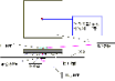
BGA temperature measurement point 
selective soldering 
AGV vehicle handling |
| Washing |
1. Solvent selection 2. Cleaning parameters 3. Concentration detection 4. Baking parameters 5. Cleaning quality 6. ESD &Temperature & Humidity control 7. Carry |
1. Cleaning fixture and fixture acceptance 2. SOP defines the operation mode of parameter 3. Inspection & process record 4. System logging 5. Surface ion concentration test 6. First article confirmation 7. Resistivity detection 8. ZESTRONA201 9. Baking time after cleaning > 8H (75℃) 10. AGV workshop 11. Electrostatic protection 12. Special tray |
Washing Place 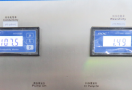
Resistivity monitoring |
| Inspection |
1. AOl program 2. SOP&Process control 3. General inspection&FQC inspection 4. ESD & Temperature & Humidity control 5. Carry |
1. 100% pass-SMT 3D AOI 2. 100% pass DIP plug-in AOI 3. 100% general inspection 4. 100% quality inspection 5. Handling by AGV vehicle 6. Equipment and personnel electrostatic protection 7. Special tray 8. System control 9. Finished product inspection report |
3D AOI |
| Packing |
1. Stress<400 u strain 2. Product anti-collision protection 3. ESD&Temperature&Humidity control 4. Burrs and dust 5. Quantity |
1. Milling cutter splitter 2. Special tray 3. Electrostatic bag,desiccant 4. Dust cleaning 5. Barcode &label control 6. System control |

depaneling machine 
Depaneling stress (max 92 u strain ) 
Packing (anti-damage & anti-static) |
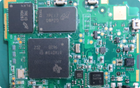
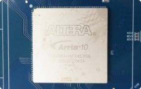
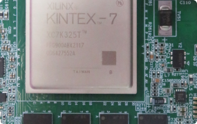
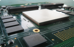
Our BGA Assembly Products Showcase


Why Choose PCBCart BGA Assembly Services?
 Standards-Driven Excellence: Every design and
assembly step aligns with IPC benchmarks.
Standards-Driven Excellence: Every design and
assembly step aligns with IPC benchmarks.
 Defect Prevention: Proactive optimization
of layouts and processes for zero-failure outcomes.
Defect Prevention: Proactive optimization
of layouts and processes for zero-failure outcomes.
 End-to-End Compliance: From design to
delivery, we guarantee adherence to your technical and
quality requirements.
End-to-End Compliance: From design to
delivery, we guarantee adherence to your technical and
quality requirements.
By integrating these standards, PCBCart ensures robust, high-yield BGA assemblies that meet the demands of cutting-edge applications. Let us turn your designs into dependable, industry-compliant solutions.
98.5%
Qualified Rate1
Time Pass99%
Satisfaction [email protected] [email protected]


