With the increasing applications of large-scale and super-large scale integrated circuits in the system of circuits, circuit boards show a development trend towards multiple layers and complexity owing to the magnifying integration scale of chips, shrinking of volume, escalation of pins and increasing of speed rate. Most of high-speed multi-layer PCBs implement connections between layers through thru-hole vias. For the electric connections that don't circulate from the top to the bottom, however, redundant thru-hole via stub will possibly take place so that PCB transmission quality will be badly influenced. Therefore, in terms of some high-speed digital systems with high performance and high requirements, the influence of redundant stubs can never be neglected. Based on the attempts to balance cost versus performance, design of blind/buried vias comes about in order to effectively avoid redundant stub effect and increase the transmission quality of systems.
With blind and buried via design as research objects and through modeling simulation, this article mainly analyzes the influence of parameters concerning via diameters of blind/buried vias, pad and antipad on signal features such as S parameter and impedance continuity and provides practical instructions to high-speed PCB blind/buried via design.
Main Parameters and Performance Index of Blind/Buried Vias
For high-speed digital circuit multi-layer PCBs, vias are necessary for high-speed signal connection between interconnection lines in one plane and interconnection lines in another plane. Vias are actually electric conductor connecting routings between different planes. Based on differences of PCB design, vias can be classified into thru-hole via, blind via and buried via, which is shown in Figure 1.

• Thru-hole vias, circulating through the whole PCB, are applied for interconnected routings between layers or as positioning vias for components.
• Blind vias, without circulating through the whole PCB, are responsible for the connection between internal layers of PCB and surface plane routing.
• Buried vias are responsible for the connection between internal layers of PCB only. They can't be seen directly from the appearance of PCBs.
Vias can't be regarded as electric connection and their influence on signal integrity has to be considered. Therefore, a better understanding of the influence of vias' architecture design on high-speed digital circuit performance is beneficial to the excellent solution to signal integrity so that design of high-speed digital system can be optimized and the transmission quality of high-speed signals can be improved.
In high-speed circuits, the equivalent electrical model of vias can be indicated as Figure 2 in which C1, C2 and L respectively refers to parasitic capacity and inductance of vias.

Based on this model, all the vias in high-speed circuits will generate parasitic capacitance to ground. Parasitic capacitance can be calculated through formula below:
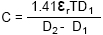
In this formula, parasitic capacitance of vias is equal to the diameter of antipad to the ground, diameter of pads of vias, dielelctric constant of substrate material and the thickness of PCB. In high-speed digital circuits, parasitic capacitance of vias makes signal's rising time become slow or declined and slows circuit speed. For a transmission line whose characteristic impedance is Z0, the relationship between parasitic capacitance and the rising time of signals can be indicated as formula below.

When high-speed signals go through vias, parasitic inductance is generated as well. In high-speed digital circuits, the influence brought by parasitic inductance of vias is larger than parasitic capacitance. Parasitic inductance can be calculated according to formula below.
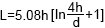
In this formula, the parasitic inductance of vias is equal to the length of vias and the diameter of vias. Moreover, the equivalent impedance caused by parasitic inductance can never be neglected and the relationship between equivalent impedance and parasitic capacitance and rising time of signals can be indicated by formula below.

Based on formulae mentioned above, the electric performance of vias changes with design parameters. The changes of via diameter, length, pad and antipad lead to impedance discontinuity in high-speed circuits with signal integrity greatly influenced. The analysis on signal features in this article lies in the indexes of S11 (return loss) and S21 (insertion loss). When the attenuation degree of insertion loss is less than -3dB, the effective bandwidth is applied to judge and analyze the signal transmission performance of blind/buried vias. Furthermore, TDR simulation can be applied to analyze the reflection caused by impedance discontinuity.
Modeling Simulation and Result Analysis of Blind/Buried Vias
To research the influence of blind/buried vias on high-speed PCB signal features, this article designs an 8-layer PCB model with HFSS software, which is shown in Figure 3 below.

In this PCB, layers 1 to 2, 4 to 5 and 7 to 8 are all signal layers; the third layer is power layer; the sixth layer is ground layer; the thickness of each layer is 0.2mm (8mil); dielectric material is FR4; dielectric coefficient is 4. The routing width of signal lines is 0.1mm (4mil), the thickness 0.13mm (1.1mil). In the simulation, the rising time of signals is set to be 20ps and the highest sweep frequency is set to be 100GHz.
• Comparison on the influence of signal features deriving from blind/buried vias and thru-hole vias
When a signal line is required to circulate from the first layer to the fifth layer, blind via can be applied for connection. The radius of blind via is set to be 0.1mm (4mil) and length to be 0.81mm (32mil).
For the sake of comparison, thru-hole via connection is designed as well with the radius of thru-hole via 0.1mm. Under this condition, the length of stub of thru-hole via is 0.6mm.
Based on the simulation result, when the frequency is in the range from 40GHz to 80GHz, the parameter of return loss of blind via (S11) is only 4dB to 7dB. However, when the frequency is in the range from 40GHz to 80GHz, the parameter of return loss of thru-hole via (S11) is only 4dB to 10dB. When the frequency is 76GHz, the parameter of insertion loss of blind via (S21) is the largest. However, when the frequency is 52GHz, the parameter of insertion loss of thru-hole via (S21) is the largest. If insertion loss is guaranteed to be less than -3dB, the operation bandwidth of blind via will be 22GHz while the operation bandwidth of thru-hole via will be only 15GHz.
In terms of characteristic impedance, the change category of characteristic impedance of blind vias is in the range from 46 to 52 while the change category of characteristic impedance of thru-hole vias is from 42 to 53, which means that blind vias have better transmission line impedance continuity. Therefore, based on the stability of S parameters and change of characteristic impedance TDR, it can be illustrated that blind vias have better transmission quality than thru-hole vias in terms of signal line connection between top layer and internal layer or between bottom layer and internal layer.
When a signal line is required to circulate from the second layer to the fifth layer, buried via can be applied for connection. The radius of buried vias is set to be 0.1mm and length if 0.57mm. Thru-hole via is also applied for comparison with its radius 0.1mil and the length of redundant stub between the first layer and the second layer is 0.23mm while the length of redundant stub between the fifth layer and the eighth layer is 0.6mm.
Based on the simulation result, when the frequency is in the range from 40GHz to 80GHz, the parameter of return loss of buried via (S11) is only 4dB to 8dB with relatively smooth change. However, when the frequency is in the range from 40GHz to 80GHz, the parameter of return loss of thru-hole via (S11) is only 4dB to 10dB. Especially when the frequency is 32GHz, the attenuation changes into 13dB instantly, influencing the stability of transmission. When the frequency is 77GHz, the parameter of insertion loss of buried via (S21) is the largest. However, when the frequency is 54GHz, the parameter of insertion loss of thru-hole via (S21) is the largest. If insertion loss is guaranteed to be less than -3dB, the operation bandwidth of buried via is 32GHz while the operation bandwidth of thru-hole via is only 20GHz.
Moreover, the change of characteristic TDR of buried via is in the range from 41.8 to 52 while the change of characteristic TDR of thru-hole via is in the range from 37.5 to 52, which means that buried via features better transmission line impedance continuity than thru-hole via. Therefore, based on the stability of S parameters and change of characteristic impedance TDR, it can be illustrated that buried vias have better transmission quality than thru-hole vias in terms of signal line connection between internal layers.
• Influence of blind/buried via diameter, pad and antipad on signal features
In order to study the influence of blind/buried via diameter, pad and antipad on signal features, the size of pad and antipad of blind/buried vias can be fixed. The initial value of radius of blind/buried vias is set to be 0.1mm and it changes within the category from 0.1mm to 0.175mm.
Based on the result of simulation, it can be indicated that when the radius of blind via changes within the category from 0.1mm to 0.175mm, the change of impedance lies in the category from 6 to 13.5 with the degree of impedance discontinuity increased that causes the increase in terms of range of insertion loss S21. When the frequency is in the range from 20GHz to 60GHz, the largest attenuation reaches 1.7dB. Meanwhile, when the radius of buried via changes within the category from 4mil to 7mil, the change of impedance lies in the category from 10 to 17 with the degree of impedance discontinuity increased that causes the increase in terms of range of insertion loss S21. When the frequency is in the range from 20GHz to 60GHz, the largest attenuation reaches 1.6dB.
With the diameter of blind via and antipad unchanged, the initial value of radius of blind/buried via pad is set to be 0.2mm and it changes within the category from 0.2mm to 0.28mm.
Based on the result of simulation, it can be indicated that when the radius of blind via pad changes within the category from 0.2mm to 0.28mm, the change of impedance lies in the category from 6.5 to 10.5 that causes the increase in terms of range of insertion loss S21. In addition, the largest attenuation increases by 2dB. Meanwhile, when the radius of buried via pad changes within the category from 0.2mm to 0.28mm, the change of impedance lies in the category from 10.5 to 15.5 with the degree of impedance discontinuity increased that causes the increase in terms of range of insertion loss S21. In addition, the largest attenuation increases by 3.2dB.
With the diameter of blind/buried via and pad size unchanged, the initial value of antipad is set to be 0.3mm and it changes within the category from 0.3mm to 0.375mm.
Based on the result of simulation, it can be indicated that when the size of blind via antipad changes within the category from 0.3mm to 0.375mm, the change of impedance lies in the category from 6.5 to 5.5 that causes the decrease in terms of degree of impedance discontinuity and range of insertion loss S21. In addition, the largest attenuation increases by 3.2dB. Meanwhile, when the size of buried via antipad changes within the category from 0.3mm to 0.375mm,, the change of impedance lies in the category from 10 to 7.5 that causes the decrease in terms of degree of impedance discontinuity and range of insertion loss S21. In addition, the largest attenuation increases by 3dB.
Conclusion
With an 8-layer PCB with blind and buried vias model established through HFSS, this article compares S parameters and characteristic impedance TDR of blind/buried vias and thorugh-hole vias. It can be concluded that blind/buried vias have smaller insertion loss and better impedance discontinuity than thru-hole vias. Under the condition that the insertion loss is less than -3dB, blind/buried vias have wider operation bandwidth than thru-hole vias.
This article also analyzes the influence of parameters including via diameter, pad and antipad on blind/buried signal features. With the increase of diameter of blind/buried vias and pad size, the attenuation of signal insertion loss shrinks accordingly and the degree of impedance discontinuity increases. However, with the increase of antipad size of blind/buried vias, the attenuation of signal insertion loss shrinks and so does impedance discontinuity accordingly.
If the insertion loss is less than -3dB and the effective operation bandwidth reaches 20GHz, the radius of blind vias should be no larger than 0.175mm and the radius of buried vias should be no larger than 0.23mm; the pad of blind vias should be no larger than 0.25mm and the pad of buried vias should be no larger than 0.275mm; the antipad of blind vias should be no smaller than 0.25mm and the antipad of buried vias should be no smaller than 0.23mm.
If the change range of impedance is controlled within ±10%, the radius of both blind and buried vias should be no larger than 0.125mm; the pad of blind vias should be no larger than 0.25mm and the pad of buried vias should be no larger than 0.175mm; the antipad of blind vias should be no smaller than 0.275mm and the antipad of buried vias should be no smaller than 0.4mm.
PCBCart Has The Capabilities to Manufacture PCBs with Blind Vias, Buried Vias and Thru-hole Vias.


