Nowadays, electronic products call for miniaturization and high accuracy so that component miniaturization has become an essential development trend. When miniaturized components are ready to be assembled on large-area PCBs, much higher requirement has to be laid to board smoothness. Naturally, it has become an essential topic for PCB manufacturers to consider how to reduce warpage extent of PCBs.
According to manufacturing regulations confirmed by IPC-600, the warpage of PCBs that are ready to go through SMT assembly is required to be 0.75% at most. When it comes to small components assembly on circuit boards with large areas, however, that regulation fails to work. Generally speaking, to meet the demands of miniaturized components assembly on PCB boards with large areas, PCB warpage should be reduced to 0.5% or lower.
Warpage Analysis
Warpage problem will be first analyzed in this part of this article with a sample 8-layer PCB whose size is 248mm±0.25x162.2±0.20. The warpage of this board is required to be 0.5% but its practical warpage after the first batch of production falls into the range from 2.5% to 3.2%.
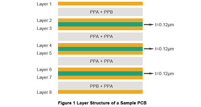
The layer structure of an 8-layer PCB is demonstrated as below.

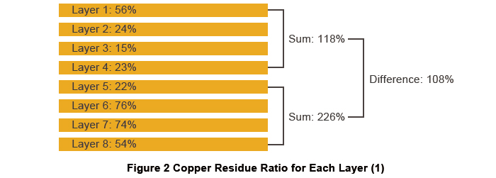
Copper residue ratio for each layer is demonstrated as the following figure.

Based on the above analysis, the protruding characteristic of this sample board is uneven copper distribution of each layer. Moreover, copper is relatively thick. As a result, board warpage is aroused.
Solutions to Defeat PCB Warpage
• Scheme#1
The primary method to balance copper residue between layers of the board lies in adding copper pouring in blank.
To reduce deformation stress of the board, it’s an agreeable idea to shrink panel size with a rotation panelization method. When it comes to this sample PCB, panel size should be modified from 610mmx520mm to 610mmx356mm. Panel array of the former is 3x2 while that of the latter is 2x2.
Due to the above measures for improvement, copper residue ratio is demonstrated in Figure 3 below. After such modifications, warpage modified to be in the range from 2.0% to 2.9% that receives obvious improvement but a little far from the requirement of 0.5%.

•Scheme#2
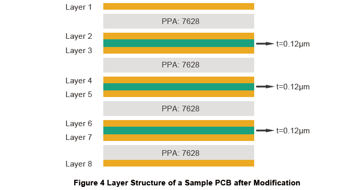
Based on Scheme#1, board rigidity is added. After such modification, the layer structure of the PCB board can be indicated by the following figure.

The implementation of this scheme makes PCB warpage in the range from 2.0% to 2.9%. Evidently, this scheme doesn’t work on warpage issue solving, indicating that there’s little correlation between warpage and board rigidity. We need to go on optimizing Scheme#1, that is, searching for more ways on copper residue balance.
•Scheme#3
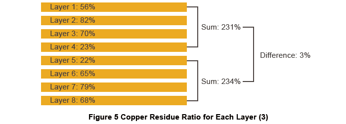
Based on Scheme#1, Layer 2 and Layer 6 should be exchanged with each other. Copper residue ratio for each layer of PCB after the application of Scheme#3 is shown as Figure 5 below.

In accordance with Scheme#3, PCB warpage remains within 0.5% and it still remains at 0.5% even after twice reflow soldering, which is compatible with demand. Furthermore, a trial production of 300 pieces verifies the reliability of this scheme. As a result, Scheme#3 performs best among all the schemes.
According to above experiments, since the distribution among all dielectric layers is even, it’s uneven distribution of copper that leads PCB warpage to occur. Through balancing copper residue on each layer of PCB board, board warpage reduces from the range from 2.5% to 3.2% to the range within 0.5%, indicating that the core solution for PCB warpage issue lies in balance on copper residue between dielectric layers and copper layers. Accordingly, as far as warpage is concerned during assembly process, equalization should be achieved by component layout, thermal distribution and assembly distribution so that board warpage can be decreased with product quality guaranteed.
With the pursuit of miniaturization and precision, PCB warpage reduction has become imperative, particularly for high-density small component boards. While IPC-600 defines warpage as 0.75%, more stringent requirements push this to 0.5%. Our research on an 8-layer PCB indicated that non-uniform copper distribution is one of the main causes of warpage. By employing focused plans, especially since Scheme #3 was successful, we were successful in minimizing warpage, underscored by the importance of sustaining copper distribution equity for maximum stability of the boards.
To ensure your boards are of high performance standards, it is important to focus on the all-critical copper distribution. Such enhancements can greatly minimize warpage, leading to improved product quality. Get a quote from PCBCart today and learn how these tailored approaches can be applied on your next project to enhance reliability and performance.
Get an Instant Quote for PCB Assembly & PCB Manufacturing
Helpful Resources
• Factors Determining the Number of Layers and Layer Distribution in PCBs
• Multilayer PCB Fabrication
• The Key PCB Design Rules You Have to Know
• PCB Design Elements Influencing SMT Manufacturing


