Impedance control technologies are quite important in high-speed digital circuit design in which effective methods must be adopted to ensure the excellent performance of high-speed PCBs.
PCB successfully added to your shopping cart
Impedance control technologies are quite important in high-speed digital circuit design in which effective methods must be adopted to ensure the excellent performance of high-speed PCBs.
• Equivalent Model on Transmission Lines
Figure 1 shows the equivalent effect of transmission lines on PCBs, which is a structure including tandem and multiple capacitor, resistor and inductor (RLGC model).

The typical value of tandem resistance is in the range from 0.25 to 0.55ohms/foot and the resistance value of multiple resistors usually remains quite high. With parasitic resistance, capacitance and inductance added in PCB transmission lines, the overall impedance on transmission lines is referred to as characteristic impedance (Z0). The value of characteristic impedance is relatively small on the condition that the line diameter is large, the line is close to power/ground or the dielectric constant is high. Figure 3 shows the equivalent model of the transmission line with a length of dz, based on which the characteristic impedance of the transmission line can be deduced as formula:  . In this formula, L refers to the inductance of each unit length on transmission line while C refers to the capacitance of each unit length on transmission line.
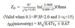
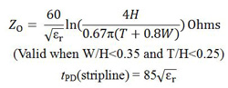
• Impedance and Delay Calculation Formula of Transmission Lines on PCB
| Transmission Lines on PCB | Impedance and Delay Calculation Formula |

|
|

|
|
In the formulae above, Z0 refers to impedance (Ohms), W refers to the width of lines (inch), T refers to the thickness of lines (inch), H refers to the distance to the ground (inch), refers to the relative dielectric constant of substrate, and tPD refers to the delay time (ps/inch).
• Impedance Control Layout Rules of Transmission Lines
Based on the analysis above, the unit delay of impedance and signal is irrelative to the frequency of signals but related with board structure, relative dielectric constant of board material, and physical attributes of routing. This conclusion is extremely important to understand high-speed PCB and for high-speed PCB design. What's more, the transmission speed of signal transmission line in outer layer is much quicker than that in inner layer so these elements must be taken into account for the arrangement of key lines layout.
Impedance control is the significant premise for the implementation of signal transmission. However, according to the board structure and impedance calculation formula of transmission lines, the impedance is only dependent to PCB material and PCB layer structure with the line width and routing features unchanged for the same line. Therefore, the impedance of a line will not change on different layers of PCB, which is not allowed in high-speed circuit design.
A high-speed PCB with high density is designed for this article and most of signals on board have impedance requirements. For example, CPCI signal line should have an impedance of 65Ohms, differential signal of 100ohms and other signals all 50ohms each. According to PCB routing space, an at least ten-layer routing must be used and a 16-layer PCB design plan is determined.
Since the overall thickness of the board can't exceed 2mm, there are some difficulties in terms of stacking with some problems considered:
1). Each signal layer has image planes adjacent to them to protect the impedance and signal quality.
2). Each power plane has complete ground layer next to them so that performance of power can be well ensured.
3). The stacking up of board requires balance, with board warpage avoided.
The dielectric constant of medium is set to be 4.3. Based on the stacking design above, line width and distance between lines should be set according to calculation result in order to ensure the requirement of signal impedance. Line width is obtained as the following result:
1). The width of signal line on the surface layer is 5mils with its impedance 58.7Ohms.
2). The width of CPCI signal line on the surface layer is 4.5mils with its impedance 61.7Ohms.
3). The width of signal line in inner layer is 4.5mils with its impedance 50.2Ohms.
4). The width of lines in BGA area in inner layer and surface layer is 4mils with surface layer impedance 64.6Ohms and inner layer impedance 52.7Ohms.
5). The width of microstrip differential line in inner layer is 5mils with the distance between lines 6mils and impedance 100.54Ohms.
6). The width of stripline differential line in inner layer is 4.5mils with the distance between lines 10mils and impedance 96.6Ohms.
Distance between lines is set as the follows:
1). The distance between signal lines (5mils) on surface layer is 5.0mils.
2). The distance between CPCI signal lines (4.5mils) on surface layer is 9.0mils.
3).. The distance between signal lines (4.5mils) on inner layer is 7.0mils.
4). The distance between lines on surface layer and inner layer is 4.0mils.
5). The distance between differential signal lines on inner layer and between them and other signal lines should be kept at least 25mils.
6). The distance between differential signal lines on surface layer and between them and other signal lines should be kept at least 20mils.
After PCB printing, the impedance of test board is tested by POLAR-Cits500 impedance tester with results in following table. The data indicates that the impedance must be controlled in the range of 50Ohmۯ%, 60Ohmۯ% and 100Ohmۯ% in the process of high-speed PCB design and fabrication.
| Pre-set Impedance (Ohm) | Practical Impedance (Ohm) |
| 50 | 47.52-52.33 |
| 60 | 57.65-61.35 |
| 100 | 93.65-106.35 |
• LVDS
LVDS is a type of high-speed serial signal transmission level with advantages of high transmission speed, low power consumption, strong anti-interference ability, long transmission distance and feasible matching. The application fields of LVDS include computer, communication and consumption.
• Impedance design of LVDS
LVDS features a voltage swing of only 350MV with the longest transmission distance of over 10 meters. In order to ensure that signals won't be influenced by reflected signal in the process of signal transmission in transmission lines, impedance of transmission lines must be under control with single line impedance 50Ohms and differential impedance 100Ohms. In the practical application, impedance can be controlled by setting reasonable stacking thickness and medium parameters, adjusting line width and distance between lines and calculating impedance of single lines and differential lines with the help of some high-speed simulation analysis tools.
However, most of the time, it's relatively difficult to meet the requirements of single-line impedance and differential impedance. On the one hand, the adjustment range of line width W and distance between lines S is controlled by physical design space. For example, the routing and line width in the margin connectors with BGA or DIP is influenced by pad size and distance. On the other hand, the change of W and S will influence the result of single line and differential impedance. Up to now, it's easy and convenient to figure out the relationship between pre-set line width and line distance.
• LVDS routing rules
Generally speaking, differential signal routing is implemented according to impedance design rules, which is capable of ensuring LVDS quality. In the practical routing, LVDS should conform to the following rules:
1). Differential pairs should be short as much as possible, lines should be straight and number of through holes should be shrinked. Distance between signal lines in differential pairs should be the same. All these rules contribute to the avoidance of long routing and numerous turning-offs. As for turning-offs, 45-degree turning-off should be used instead of 90 degrees.
2). Distance between differential pairs should be maintained over 10 times in order to decrease the crosstalk between lines. When necessary, ground through holes can be placed between differential pairs for isolation.
3). LVDS can't be split across surface. Although two differential signals are mutual returning paths, signal returning path can't be cut down as a result of across-surface splitting. Nevertheless, transmission lines will possibly lead to impedance discontinuity as a result of a lack of image planes.
4). Avoid differential signal between layers. During PCB manufacturing, stacking alignment accuracy between layers is much lower than etching accuracy in the same layer plus the medium loss during stacking, all of which leads to the change of differential impedance between differential pairs.
5). In impedance design, coupling method should be used in it.
6). Suitable PCB stacking structure should be set to ensure the isolation between voltage level signals and LVDS. When possible, signals such as high-speed TTL/CMOS can be set on different layers, isolated from LVDS routing by ground and power layers.
7). Differential signal pairs should be compatible with the length of routing.
Helpful Resources
• Elements Affecting Characteristic Impedance of PCB and Solutions
• Impedance Design Considerations for Flex-Rigid PCB
• How to Analyze and Prohibit Impedance of High-Speed PCB Power
• Impedance Control of Vias and Its Influence on Signal Integrity in PCB Design
• Full Feature PCB Manufacturing Service from PCBCart - Multiple Value-added options
• Advanced PCB Assembly Service from PCBCart - Start from 1 piece


