Vias play a role as conductors connecting traces across different layers of a multi-layer PCB (Printed Circuit Board). In the case of low frequency, vias don't affect signal transmission. As frequency rises (1GHz above) and signal rising edge becomes steep (1ns at most), however, vias can't be simply regarded as a function of electrical connection but influence of vias on signal integrity has to be carefully considered. Vias behave as breakpoints with discontinuous impedance on transmission line, causing signal reflections. Nevertheless, issues brought by vias concentrate more on parasitic capacitance and parasitic inductance. The influence of via parasitic capacitance on circuit is primarily to prolong the rising time of signals and reduce the running speed of circuit. Parasitic inductance, however, can weaken the contribution of bypass circuit and decrease filtering function of the whole power system. This article will demonstrate how via impedance control affect signal integrity and provide some advice on circuit design.
Influence of Vias on Impedance Continuity

According to TDR (time domain reflectometer) curve at time of via presence and via absence, obvious signal delay does occur at the situation of via absence. In the case of via absence, the time span of signal transmission to the second test hole is 458ps while that of signal transmission to the second test hole is 480ps in the case of via presence. Thus, via leads signals to delay for 22ps.
Signal delay mainly results from parasitic capacitance of vias that is figured out through the formula below:
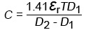
In this formula, D2 refers to pad diameter (mm) on the ground, D1 to pad diameter (mm) of via, T to PCB board thickness (mm), εr to dielectric constant of substrate and C to parasitic capacitance (pF) of via.
The length of via in this discussion is 0.96mm with via diameter 0.3mm, diameter of pad 0.5mm and dielectric constant 4.2 with which involved in the formula mentioned above, the calculated parasitic capacitance is figured out to be approximately 0.562pF. When it comes to a signal transmission line with resistance of 50Ω, this via will cause changes in rising time of signals with the change amount figured out by the following formula:
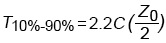
Based on the formula introduced above, rising time variation caused by via capacitance is 30.9ps that is 9ps longer than tested result (22ps), indicating that a variation does occur between theoretical result and practical result.
In conclusion, signal delay caused by via parasitic capacitance isn't so obvious. As far as high-speed circuit design is concerned, however, attention should be highly paid to especially layer conversion with vias multiply applied in tracing.
Compared with parasitic capacitance, parasitic inductance featured by vias leads to more damage to circuit. Parasitic inductance of vias can be figured out by the following formula:
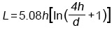
In this formula, L refers to parasitic inductance (nH) of via, h to length (mm) of via and d to via diameter (mm). Equivalent impedance aroused by via parasitic inductance can be figured out by the following formula:
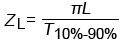
Rising time of test signals is 500ps and its equivalent impedance is 4.28Ω. But impedance change as a result of vias reaches more than 12Ω and it indicates that measured value features extreme variation with theory-calculated value.
Influence of Via Diameter on Impedance Continuity
In accordance with a series of experiments, it can be concluded that the larger via diameter is, the more discontinuity via will cause. In high-frequency and high-speed PCB design process, impedance change is usually controlled within the range of ±10%, or signal distortion is possibly generated.
Influence of Pad Size on Impedance Continuity
Parasitic capacitance features extremely large influence on resonance points within high-frequency signal band and band width will suffer from shift along with parasitic capacitance. The leading element affecting parasitic capacitance is pad size that features equivalent influence on signal integrity. Thus, the higher pad diameter is, impedance discontinuity it will bring forward.
When pad diameter changes within the range from 0.5mm to 1.3mm, impedance discontinuity caused by vias will become constantly reduced. When pad size increases from 0.5mm to 0.7mm, impedance will feature relatively large change amplitude. As pad size keeps rising, via impedance change will become smooth. Therefore, the larger pad diameter is, the lower impedance discontinuity aroused by vias will be.
Return Path for Via Signals
Basic principle of return signal flowing is that high-speed return signal current runs along the lowest inductance path. Since a PCB board contains more than one ground plane, return signal current runs directly along one path below signal lines at the ground plane that is the nearest to signal line. When it comes to the situation when all signal currents from one point to another flow along the same plane, if signals are made go from one point to another through a via, return signal current won't be able to jump when ground connection isn't achieved.
In high-speed PCB design, return path can be provided to via signal current to eliminate impedance mismatching. Around via, grounding via can be designed to provide return path for signal current with an inductance loop generated between signal via and grounding via. Even impedance discontinuity comes into being due to the influence of vias, current will be able to flow towards inductance loop with signal quality improved.

Signal Integrity of Vias
S parameters can be used to evaluate the influence of vias on signal integrity, representing properties of all ingredients in the channel including loss, attenuation and reflection etc. In accordance with a series of experiments leveraged in this article, it's indicated that grounding via is capable of reducing transmission loss and the more grounding vias become around vias, the lower transmission loss will be. Grounding via adding around vias is capable of decreasing loss caused by vias to some extent.
According to the discussion demonstrated above in this article, two conclusions can be made:
a. Impedance discontinuity caused by vias is affected by via diameter and pad size. The larger via diameter and pad diameter become, the more serious aroused impedance discontinuity will be. Impedance discontinuity caused by vias usually goes down as pad size rises.
b. Grounding vias adding is capable of evidently improving via impedance discontinuity that can be controlled within the range of ±10%. Moreover, grounding vias adding can also evidently increase signal integrity.
Need PCB Fabrication Service with Strict Impedance Control? PCBCart Can Do That!


