In order to be compatible with the development requirement like miniaturization, digitalization, high frequency and multiple functions, metal wires on PCBs (Printed Circuit Boards) as interconnect devices in electronic equipment not only determine the opening of current flow, but also play a role as signal transmission lines. In other words, electrical test implemented on PCBs responsible for transmitting high-frequency signals and high-speed digital signals has to confirm the on, off and shortcut of circuits on the one hand. It also should determine that characteristic impedance must never go beyond regulated range on the other hand. One word, a circuit board will never achieve conformance to requirement unless both requirements are met.
Circuit performance provided by PCBs has to ensure reflection won't take place during signal transmission process; signals keep integrated; transmission loss be reduced with impedance matching achieved. Consequently, transmission signals can be achieved integrally, reliably and accurately without interference or noise. This article focuses on characteristic impedance control of multilayer boards with microstrip structure.
Surface Microstrip and Characteristic Impedance
With high characteristic impedance, surface microstrip has been widely applied in PCB fabrication. A signal plane is set to be outer layer controlling impedance and insulating material used to separate the signal plane and its adjacent datum plane, which can be clearly seen in the image below.

Characteristic impedance can be figured out through formula: 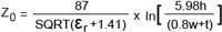 .
.
in which Z0 refers to the characteristic impedance; εr to dielectric constant of insulating material; h to the thickness of insulating material between traces and datum plane; w to the width of traces; t refers to the thickness of traces. The figure below clearly demonstrates the meaning of each parameter.
Based on the formula displayed above, it can be concluded that elements affecting characteristic impedance include:
a. Dielectric constant of insulating material (εr);
b. Thickness of insulating material (h);
c. Width of traces (w);
d. Thickness of traces (t).
It can be further concluded that characteristic impedance is closely related with substrate material (CCL material). Thus, lots of considerations have to be taken into substrate material selection.
Dielectric Constant and Its Effects
Dielectric constant of material is measured by material manufacturers when frequency falls under 1MHz. Even the same type of material may differ from each other when they are produced by different manufacturers owing to different resin content. Take epoxy glass cloth as an example. Relationship between dielectric constant of epoxy glass cloth and frequency can be summarized into the following figure.

Obviously, dielectric constant goes down as the improvement of frequency. Therefore, dielectric constant of insulating material should be determined according to the operating frequency of material and average value is capable of meeting ordinary requirement. Transmission speed of signals will decrease as dielectric constant rises, so dielectric constant has to be decreased if a high signal transmission speed is demanded. Furthermore, high characteristic impedance has to be ensured for sake of a high transmission speed, which then depends on material with low dielectric constant.
Width and Thickness of Traces
Trace width is one of the most influential elements affecting characteristic impedance and Figure 4 below demonstrates the relationship between characteristic impedance and trace width.

Based on Figure 4, it can be concluded that as trace width changes by 0.025mm, impedance will be thereafter changed by 5 to 6 ohm. In practical PCB manufacturing, however, if copper foil with width tolerance of 18μm is selected as signal plane to control impedance, the allowable trace width tolerance is ±0.015mm. If copper foil with width tolerance of 35μm is selected, the allowable trace width tolerance is ±0.003mm. In conclusion, trace width change will lead to dramatic change of impedance. Trace width is designed by designers based on multiple design requirements and it should not only meet the demand of current capacity and temperature rise, but lead impedance to an expected value. Therefore, trace width must be ensured to be compatible with design requirement and within allowable tolerance.
Trace thickness also needs to be determined according to required current capacity and allowable temperature rise. In manufacturing, coating thickness is generally 25μm in average. Trace thickness is equal to sum of copper foil thickness plus coating thickness. It should be noted that trace surface must be cleaned up prior to electroplating so that contaminant can be eliminated. Otherwise, trace thickness will possibly suffer from unevenness, which then affects characteristic impedance.
Thickness of Insulating Material
Based on the formula introduced above figuring out characteristic impedance, it can be concluded that characteristic impedance is directly proportional to the natural logarithm of thickness of insulating material (h). Thereafter, the larger "h" becomes, the larger "Z0" will be. Thus, insulating material thickness is also a crucial element determining characteristic impedance. Since trace width and dielectric constant of material have been determined prior to manufacturing and trace thickness can be regarded as a solid value, it is a primary method to control characteristic impedance through controlling lamination thickness. Relationship between trace thickness and characteristic impedance can be summarized into the following figure.

From this figure, it can be indicated that as thickness rises by 0.025mm, characteristic impedance will be changed by 5 to 8ohm. However, in PCB manufacturing process, huge change will possibly be caused by a change of each laminate thickness. As a matter of fact, prepreg with different types is selected as insulating material in manufacturing and thickness can be determined by the number of prepreg. Take microstrip as an example. Figure 3 can be used to determine dielectric constant of insulating material based on corresponding working frequency, after which characteristic impedance can be figured out. Afterwards, in accordance with trace width and calculated value of characteristic impedance, Figure 4 can be used to figure out thickness of insulating material, based on which type and count of prepreg can be deduced based on the thcikness of CCL and copper foil.
In accordance with Figure 5 above, it is shown that microstrip structure features higher characteristic impedance than stripline structure with insulating material with the same thickness applied. As a result, microstrip structure is the preference of high-frequency and high-speed digital signal transmission. Furthermore, characteristic rises with the improvement of thickness of insulating material. Consequently, when it comes to high-frequency circuits with strict characteristic impedance, CCL insulating material thickness has to maintain a stringent tolerance that is usually 10% at most. For multi-layer boards, however, insulating material thickness is a manufacturing parameter as well, so it should be also strictly controlled.
In conclusion, even a slight change in terms of trace width, trace thickness, dielectric constant and thickness of insulating material can lead to a change on characteristic impedance. Apart from those elements, it is closely related with more elements. Therefore, it's of significant necessity for manufacturers to be fully aware of elements arousing changes of characteristic impedance and adjust manufacturing parameters so that charateristic impedance can be kept within an acceptable range.
PCBCart is capable of manufacturing printed circuit boards with impedance tolerance controlled in the range of ±5% - ±10%. Want to know how much it cost to bring your custom design into real boards? Use our online PCB price calculator to get your PCB price within seconds.
Get an Instant Quote for PCB Assembly & PCB Manufacturing
Helpful Resources:
• Impedance Control in PCB Design of High-Speed Digital Circuit
• Impedance Control of Vias and Its Influence on Signal Integrity in PCB Design
• Impedance Design Considerations for Flex-Rigid PCB
• Full Feature PCB Manufacturing Service from PCBCart - Multiple Value-added options
• Advanced PCB Assembly Service from PCBCart - Start from 1 piece


