The new generations of electronic technologies lead to increasing high edge speed of components. The improvement of working speed of circuit causes increasingly high requirements on PCB design. The quality of PCB design even determines the working performance of components and the whole circuit. Especially with cost and PCB area and functionality of comprehensive circuit considered, the sources of EMI (Electromagnetic Interface) generation become increasingly wider with complicated mechanism.
EMI Mechanism and Solutions
The main elements of EMI contain electromagnetic interference source, transmission route and interfered object. With elements leading to the advent of EMI specified, it is necessary to determine elements that are easy for resolution and those that can only be partially solved in the process of PCB design so that they can be taken into consideration in the process of layout, routing and grounding.
• Layout
In terms of PCB layout, areas should be divided according to different functionalities. Different functionalities are distributed into different areas while special attention has to be paid to sensitive units in function areas.
Generally, the following principles have to be followed for PCB layout:
a. In high-speed circuits, parameters of pin distribution of components have to be considered and the distributed capacity of component pins is quite essential especially for high-speed clock signals. Meanwhile, distributed inductance has to be taken into reference since it will possibly lead to oscillation of signals, which causes circuit function failure. Therefore, in the process of layout, distribution has to be arranged with high density with lead length lowered for future routing and the influence of EMI decreased.
b. If both analog components and electronic components stay in a circuit, they have to be distributed independently in the process of layout. Since signals of digital components have complicated composites with multiple harmonic waves existed, great influence will be generated to analog signals. So they have to be considered with great care.
c. Clock units are essential in high-speed circuits. The working mechanism of clock unit is actually equivalent to a noise source, which means this unit will be oscillated when certain conditions are met. As an important source of conductivity interference and radiation interference, clock unit mustn't be placed at the edge of PCB. Otherwise, EMI would become so serious. It is necessary to place clock units at the center of PCB, which can greatly reduce EMI in circuits.
• Routing
In the process of PCB routing, under the circumstance of low cost, ground plane can be enlarged as much as possible in order to decrease the influence of EMI. However, in the circumstance where cost should be strictly controlled, the number of layers of PCB and stack sequence has to be considered carefully. Moreover, signal types have to be considered and routing has to be independently carried out to high-speed signals and low-speed signals. In addition, other elements have to be considered including source of noise and how to strengthen noise inhibition, issues on impedance matching (High-speed signals without suitable matching will definitely lead to reflection of signals and decrease the reliability of circuits), and net list.
a. Basic principles of routing
The general principles that are followed in routing include:
1).Breakpoints should be avoided in routing, which means that right angle should be avoided, as is shown in Figure 1 below.

Since right angle will possibly lead to reflection, inflection point should be designed smoothly to avoid this phenomenon. Simultaneously, key signals mustn't be beyond divided areas, or EMI will be instantly enhanced. The most common signal bypassing is to cross different power divided areas.
2).In the process of layout, analog components and digital components are required to be divided from each other, which means that routings of them should be divided. Simultaneously, the width of ground wires and power wires should be enlarged with the general rule that the width of ground wires is larger than that of power wires that is larger than that of signal wires. Moreover, 3W principles should taken into full consideration on the routing of signal wires while for multi-layer boards, 20H principle should be considered on internal layers. The completion of the work above is capable of avoiding 70% of EMI. In terms of analog sensitive wires, measures can be implemented such as grounding.
3).For the routing of USB2.0 or other high-speed differential lines, coupling routing should be applied and the integrity of reference surface between differential pairs should be guaranteed. Since differential pairs are generally high-speed signals, routing shouldn't be arranged at the edge of PCB.
b. Loops
Loops can never be avoided in PCB design. Loops are formed from signals flowing out to flowing into and each of loops plays a role as an antenna in functionality. To reduce EMI in PCB, both the number of loops and antenna capability of loops should be decreased. It means that the flow direction of each signal should be aware in PCB design and loop area has to be decreased for high-speed signals.
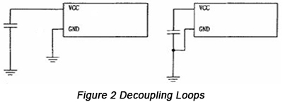
In circuits, the most commonly-used loops lie in power loops contained by decoupling capacitor, as is shown in Figure 2.

If decoupling capacitor is placed as the left diagram in Figure 2, relatively large current loops will be generated with obvious EMI phenomenon. In contrary, in the right diagram of Figure 2 in which decoupling capacitor is placed closely next to chip, an extremely small decoupling loop is generated with a main functionality of reducing EMI. The principles that should follow are displayed to reduce loops:
1).Only one path is ensured between two points on each signal line.
2).Ground plane should be applied with no block in signal loops ensured.
c. Ground wires of PCB
1).Differences should be clarified between digital ground, analog ground, and system shield ground in the system of PCB grounding. Magnetic beads and capacitor are applied to separate digital ground and analog ground and digital ground and field ground should be directly connected.
2).If allowable, ground wires should be widened in PCB.
3).Form closed circuits by ground wires so that anti-interference capacity will be strengthened and electric level difference reduced between systems.
• Filter design
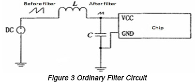
In high-speed PCBs, filter processing can be implemented on power wires and signal wires. The common measures include addition of magnetic filter components, EMI filter and decoupling capacitor.

a. Selection of decoupling capacitor
1).In a circuit, decoupling capacitor helps make power smooth and strengthening anti-interference capacity. Generally, ceramic capacitor is picked up as a decoupling capacitor owing to its high stability, high accuracy, small volume and low ESR (Equivalent Series Resistance). In circuit design, the value of resistance is chosen in the range from 1μF to 100μF while the capability of withstanding voltage has to be considered according to circuits.
2).Decoupling capacitor has to be placed closely next to components.
b. Selection of magnetic components
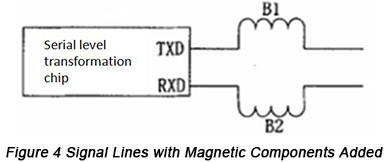
Magnetic components can be classified into inductor and magnetic beads. Generally, inductor is picked up at the end of power terminal while magnetic beads between signal lines. In the process of component selection, the saturation parameters have to be taken into consideration. Once magnetic components reach saturation, they'll be burned down. Furthermore, both quality and DCR parameters of magnetic components have to be considered.
Commonly-used measure among signal lines lies in the application of magnetic beads on serial lines to strengthen EMI capacity.

c. Selection of EMI filter
The area with serious common mode interference lies in the place with power in and signal lines out. Ordinary measures to avoid common mode interference include the addition of common mode inductor, piezoresistor, LC circuit and specific EMI filter. In high-speed circuits, EMI problem has to be considered for the high-speed transmission on digital interfaces such as USB and HDMI.
• Signal reflection
In signal transmission, energy at the source terminal is always expected to be transmitted to loading terminal, which means that ZL should be equal to ZO. If they are not equal to each other, part of energy will be reflected.
If transmission delay of lines is relatively long, stronger signals will be reflected back to source terminal. Then a relatively big amount has to be changed for compensation when ringing is generated, which is shown in Figure 5 below.

When ringing takes place to signals, EMI reaches the peak of severity. To avoid such phenomenon in PCB design, please follow principles in Table 1.
|
Signal edge time (ns)
|
Length of signal lines (inch)
|
|
5 |
8.6 |
|
4 |
6.9 |
|
3 |
5.1 |
|
2 |
3.4 |
|
1 |
1.7 |
EMI Test
After product design, in spite of a lot of measures to avoid EMI, problems won't be found until the implementation of test. Then, some modifications can be made to solve problems.
EMI test includes test method, devices and test position. Test methods should be carried out with reference of all items. If devices fail to reach the standard, a spectrometer can be applied for qualitative test. If specific EMI value of devices is required, professional devices have to be applied. As for test position, it's best to do the test in darkroom.


