Nowadays have witnessed wide applications of RF/Microwave PCBs in numerous handheld wireless devices and commercial industries including medical, communication, etc. Since RF (radio frequency)/Microwave circuits are distributed parameter circuits that tend to generate skin effect and coupling effect, interference and radiation in circuits are difficult to control in practical printed circuit board (PCB) design. The commonly occurred issues include cross-interference between digital circuit and analog circuit, noise interference caused by powers, and similar interference issues caused by absurd layout. As a result, how to balance advantages and disadvantages in PCB design and try to shrink interferences is a crucial aspect for RF/Microwave PCB design.
Every design differs, but experience plays an active role as a great teacher and the manufacturing engineer is capable of providing solutions to the major pitfalls. Detailed PCB design guidelines concerning RF/Microwave PCBs will be introduced and discussed in this article.
How to determine substrate materials?
As an early stage in circuit design, PCB substrate material selection plays such a key role in RF/Microwave PCB design that optimal substrate material contributes to excellent performance and high reliability of end products. When considering substrate material in conformity with your PCB design, some aspects have to be focused like relative permittivity, loss tangent, thickness, environment etc. The following content will detail their significance and ideal selection approaches will be displayed.
• Relative Permittivity
Relative permittivity refers to the ratio between dielectric constant and vacuum permittivity. Relative permittivity of substrate materials applied for RF/Microwave PCB design must be sufficiently high to meet demands of space and weight. Other applications such as high-speed interconnect, however, call for extremely low relative permittivity to produce high-impedance circuits with acceptable line width and impedance tolerances.
In advance of final substrate materials determination, some parameters have to be confirmed including line width for a certain range of board thickness, wavelength of circuit working frequency and approximate dimensions of leading components. A sketch of circuit board diagram has to be drawn in order to establish acceptable maximum and minimum relative permittivity.
Moreover, relative permittivity deviation provided by substrate material manufacturer has to be low enough to make electric performance within a tolerance range.
• Loss Tangent
Dielectric loss is a function concerning loss tangent and relative permittivity. As for some substrate materials, dielectric loss per unit length can possibly be offset by application of shorter lines that can reduce conductor loss as well, which is vitally important when conductor loss becomes obvious in high-frequency situation. Thus, when parameters of component loss in some circuits are being estimated, it is loss per unit length or frequency that is estimated instead of ordinary loss per unit line length under given frequency.
Within a certain frequency range, substrate material loss has to be low enough in order to meet input/output power requirements with heat dissipation issues avoided. Furthermore, power response of some circuit elements (such as filters) has to maintain a sharp frequency roll-off characteristic so that electric performance requirement can be met. Naturally, dielectric loss can impact this frequency characteristic.
• Thickness
Substrate material thickness is associated the following design elements:
a. Trace width. To maintain given characteristic impedance, substrate material thickness should be reduced to meet the requirement of trace width decrease. High-impedance trace on thin substrate material perhaps needs extremely low trace width when it comes to manufacturing.
b. Mechanical Performance. Circuits constructed on unsupported thin substrate material may bow, warp or distort, which won't possibly happen to rigid and thermoset materials.
c. Size Stability. Generally speaking, thin substrate materials perform worse than thick ones in terms of size stability. Plus, thin substrate materials will also bring about setbacks to manufacturer or lead to increased cost.
d. Cost. Generally, substrate materials that are thick per unit area are more costly than those that are thin per unit area.
e. Conformability. For circuit boards that are needed to bend into simple bending shapes such as cylinder or cone, thin boards are capable of bending to lower curvature radius with substrate materials or copper foil stopped from being destroyed.
f. Dielectric Breakdown. For parallel boards, thin dielectric material features proportionally higher dielectric breakdown voltage than thick material.
g. Power Handling Capability. Power handling capability of high-frequency circuit boards are limited by two aspects that can be alleviated by adding substrate material thickness. On one hand, high power can be partially dissipated through heat. On the other hand, high-peak power level can lead corona inception to generate electricity and shrink life span of substrate material.
• Environment
Printed circuit board fabrication and operational environment keep constraints to substrate material selection. The main material performances that should be taken into consideration include:
a. Temperature Stability. Operational and technical highest and lowest temperature should be guaranteed and temperature limit should be indicated as "peak" or "continuous". Electric performance modification should be calculated in peak temperature and compared with design requirement. Circuit boards won't possibly be made work during the range of intermittent temperature peaks so "continuous" temperature should be applied to estimate performance. Permanent damage occurred on mechanical performance of circuit board should be checked in "intermittent" limit temperature range.
b. Humidity Resistance and Chemical. Substrate materials should absorb low amount of humidity so that electric performance of circuit board won't be obviously decreased in high-humidity environment. After all, extra environmental protection solutions arouse extra manufacturing cost and design compromise. To-be-used techniques need to be compatible with chemical resistance and solvent resistance of substrate material.
c. Anti-Radiation Performance. When RF/Microwave PCBs are applied in space or nuclear applications, substrate materials will suffer from massive ionizing radiation. Influence on substrate mechanical and electric performance by ionizing radiation should be ensured and estimated. Moreover, its accumulative effect should be ensured and effective operation lifespan of circuit board should be compared with that.
• Other Design Rules Concerning Substrate Material
a. Adhesion of copper coil must be high enough to withstand application and manufacturing environment so as not to cause permanent damage.
b. Relative permittivity changes with temperature, which will possibly influence electric performance within working temperature range.
c. Reliability of surface mount devices (SMDs) and plated-through holes (PTH) is associated with CTE as well.
d. Thermal conductivity of substrate material will affect design with thermal management issue considered.
e. When deciding housing and mounting, board warpage should be considered in advance.
f. Mechanical performance will probably affect assembly and mounting design.
g. Specific gravity of substrate material determines weight of circuit board.
h. Coefficient of thermal expansion (CTE) has to be carefully considered in the process of limit environment temperature and high-power components designing and application of reflow soldering or other high-temperature manufacturing.
i. Electrical resistivity will probably be an element associated with electrical performance, especially when high-impedance lines transmit high voltage, power amplification circuit, for example.
How to process electrical characteristics?
Crucial high-frequency electrical characteristics contain characteristic impedance (Z0), attenuation coefficient (α) and signal transmission speed (v). Characteristic impedance and signal transmission speed are determined by effective relative permittivity while signal loss by attenuation coefficient.
Among all possible transmission structures, such as stripline (definition of stripline will be introduced in Section a below), microstrip, bipolar pulse or groove, stripline and microstrip are most widely applied in microwave circuit design and generally depend on soft base material. For either stripline or microstrip, ratio between ground distance and conductor width, conductor thickness and distance between coupling conductors strongly influences characteristic impedance and attenuation coefficient. Within a certain frequency range and on a structure of transmission line, attenuation coefficient, relative permittivity and characteristic impedance may feature frequency dependability.
When cross-section size of stripline or mircrostrip is larger than wavelength in dielectric, other (higher) transmission mode becomes significant, which makes electrical performance of transmission lines weakened. As signal speed and frequency rise, dimensions of transmission lines must be proportionally decreased to avoid higher order modes, requiring application of thinner substrate materials with given characteristic impedance maintained.
• Stripline
Stripline is a transmission line structure, including a signal line and two wider grounds that are parallel to the signal line that is clamped between. The figure below demonstrates a typical stripline in a sectional view excerpted from IPC-2252.
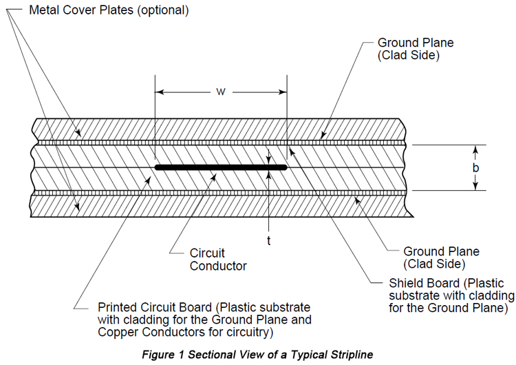
Formula for characteristic impedance of stripline are classified into two aspects: narrow signal lines and wide signal lines.
a. Narrow signal lines
Z0 refers to characteristic impedance (ohms);
εr refers to relative permittivity;
b refers to distance between grounds (m);
w refers to signal line width (m).
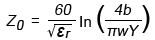
Value of Y caters to formula: 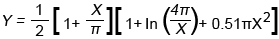
In this formula,  , t refers to copper thickness (m).
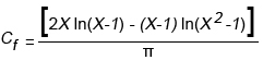
b. Wide signal lines
In this formula, Cf refers to fringing capacitance and conforms to the following formula:

• Asymmetric Stripline
When signal line is placed among grounds (or powers) but not at the central position, calculation formulae of stripline have to be modified. In the process of modification, it's necessary to coupling differences between signal lines and nearer and further grounds. If signal lines lie in the range of one third of center, deviations aroused by the assumption that signal lines lie in the center will be very small.
When coupling is highly required between signal lines, asymmetric stripline structure has to be depended, compromising two signal lines that are located in different surfaces and separated by dielectric. Coupling is carried out through parallel lines or crossing lines. When it comes to high-frequency circuit design, coupling isn't needed, the structure of vertically crossing signal lines doesn't work.
• Microstrip
Microstrip is also a type of transmission line structure, including a signal line and ground that is parallel to the signal line.
Characteristic impedance formula of microstrip is based on a simple model of microstrip containing only one dielectric that is a conductor with none thickness. The formula goes like Formula 7
In this formula, formula 8, the second "0" and "1" after Z refers to denote zero conductor thickness and a type of dielectric. Thus, the accuracy of this model is better than 0.01% when the value of u is less than 1. When the value of u is less than 1000, the accuracy is better than 0.03%.
How to arrange other significant aspects?
• Machined Features
a. Dimensions and Tolerances
Among designing elements, dimension and tolerance design are vitally important. In field designing, bilateral tolerancing and true-position tolerancing are usually applied.
True-position dimensions and tolerances that are simply marked make manufacturers arrange deviations within positions and dimensions at any proportion, which usually leads to increased manufacturability. As a result, designers ensure functionality requirements and provide manufacturers sufficient freedom by which leading deviation can be arranged in the manufacturing process where accuracy is the lowest.
Position tolerance capacity mainly depends on material type, thickness and overall size of components. A true-position diameter of 0.254mm (0.01inch) is the most commonly seen and the easiest to be obtained. When tolerance requirement is required to be higher than 0.152mm (0.006inch), manufacturability will be compromised. When it is suitably required, however, the maximum material condition should be required to allow manufacturers to balance between aperture error and position error to increase manufacturability.
When a via is manufactured according to its minimum diameter, true-position tolerance is required to be used by maximum material condition that is simply marked. Nevertheless, via manufactured by a larger and acceptable diameter is usually positioned with lower accuracy, which still ensures to be fit and function. Thus, larger vias can get sufficient position tolerance, equal to acceptable adding value to diameter of minimum via. With extra tolerance added to true-position tolerance, inspection tolerance is generated.
When minimum material condition is applied, tolerance is established according to maximum diameter. "Regardless of feature size" refers to application of mark tolerance without extra tolerance and characteristic dimension tolerance is determined according to acceptable different manufacturabilities.
Although both true-position dimension and tolerance can be applied in any case that can be imagined, they are best applied to features similar to positions of hole, pockets and the other X and Y axis.
b. Plated-Through Holes
Minimum aperture diameter is determined by thickness of the whole material. Aspect ratio is usually applied to indicate a difficulty coefficient, which is ratio between material thickness and aperture diameter. For example, when aspect ratio is 5:1 and stripline circuit board features thickness of 3.3mm (0.13inch), it demonstrates that the minimum aperture diameter is 0.66mm (0.026inch).
Generally speaking, an aspect ratio of approximately 3 is easier to be manufactured while 5 is more difficult and 10 is extremely difficult and sometimes even fails to be manufactured. Simply put, plated-through holes with high aspect ratio tend to be manufactured more easily on thin material while drilling holes with high aspect ratio tend to be manufactured more difficultly. When it comes to drilling holes with a diameter smaller than 0.33mm (0.013inch), broken drill and via roughness will be a practical issue. Moreover, holes with high aspect ratio are difficult to be cleaned, activated and metalized. Due to dispersibility of solution, metallization is distributed unevenly inside a hole. Limited dispersibility reduces material transmission of atoms and molecules inside holes and makes original current distribution of plating become complex.
Hole diameter can be regulated to be prior to metallization and post metallization. Metallization makes hole diameter shrink two-fold plated thickness. Aperture error after metallization is limited by error that occurs during hole drilling and metallization. Although more rigorous tolerance can be achieved, a tolerance zone of 0.13-0.25mm (0.005-0.01inch) is the most commonly seen. Generally speaking, cost and difficulty level rise with the reduction of aperture diameter tolerance. An empirical rule says: if aspect ratio is larger than 4:1, via diameter should be increased to 0.10mm (0.04inch) or more.
Aperture diameter through metallization fails to be accurately forseen owing to plated current density distribution. Difference in terms of local current density leads metalized thickness to be influenced by aperture diameter, hole density, ambient circuit and ground shape. Generally, hole dimension prior to metallization and minimum metallization thickness are regulated to increase manufacturability. When plated-through holes prohibit ground or internal interconnection as a mode, it's suitable to determine minimum plated-through hole. When holes are regarded as lead components, bilateral tolerance should be considered in hole dimensions.
When electroplated tin/lead needs to be fused or reflowed, hole dimensions have to be indicated as those prior to reflow soldering. In the stage of reflow soldering, each detail of design like pad dimension, hole dimension and material thickness and circuit thickness will affect flowing of solder and dimensions after reflow soldering. Plated-through holes after modular limitation can't partially or wholly closed by metal.
• Metalization
a. Plated Edge Designs
In multilayer PCBs, plated edging has been an acceptable technology in order to reduce mode suppression plated-through holes. Plated edge design should contain three to four 6.4mm (0.25inch)-wide connectors that are responsible for connecting tabs on the whole board. As a result, numerous tabs can be manufactured as a whole board form. Plated edging has to overlap width of at least 1.3mm (0.050inch) of top layer or bottom layer so as to stronger mechanical adhesion. Thickness of metallization should be at least 0.025mm (0.001inch).
b. Copper Plating
Prior to plating, all metal surface and exposed dielectric are covered with a layer of coating without electro-plating or conductivity. Then necessary thickness of copper should be plated on the whole board or graphics.
Generally speaking, panel plating is an optimal selection if thickness uniformity is rigorously required. After all, image won't affect plating distribution. Furthermore, when thick metallization is needed, panel plating is capable of sinking a large amount of metal with bridging not formed between images. Conversely, image plating can only be regarded as an optimal selection when trace width/spacing tolerance requires high strictness because copper foil that needs to be etched off is brought together by substrate material with the same level of thickness.
Mechanical performance of plating copper determines thermal shock resistance and thermal cycle resistance of plated-through hole. In the process of soldering assembly and environmental temperature circulation, cracks are possibly generated to plated-through holes. Copper has to be with sufficient malleability to withstand the shock of high temperature and to resist fatigue failure caused by lower environmental temperature. When it comes to high reliability, acid plating copper system is suggested being applied by PCB manufacturers since plating copper is capable of reaching malleability of at least 20% and tensile strength of at least 2.76x10⁸Pa.
Plating thickness usually decides minimum thickness of plated-through hole wall that is usually regulated to be 0.0025mm (0.001inch). Remember hole wall of 0.0025mm (0.001inch) will cause a thickness of 0.004-0.005mm (0.0015-0.002inch) of other surfaces. If image plating soldering technology isn't applied, plating thickness will exceed 0.05mm (0.002inch), arousing issues concerning corrosion accuracy.
In panel plating and image plating, types of holes influence metal distribution. Independent holes receive faster soldering than dense holes. Thickness uniformity level of metal on components is determined by the percent of metal covered in plating area. When holes and image are not evenly distributed, thickness tolerance will be larger. A typical plating copper thickness is ±0.013mm (0.005inch). Once tolerance is ±0.005mm (0.0002inch) or lower, manufacturability will be reduced.
If metallization thickness or the overall thickness of end product is regulated, tolerance should be a sum of plating tolerance and copper foil thickness and/or dielectric tolerance. Thickness of copper foil is determined by copper weight per unit area.
RA copper foil features a lower thickness tolerance than electrolytic copper foil. Therefore, some slight changes take place on copper foil thickness but requirements can still be met. It has been found that thickness changes to ±0.005mm (0.0002inch) on 0.5 to 1oz copper foil.
The overall metallization thickness is obtained through microscopic analysis after polishing and corrosion. Internal sample is placed around components and will be cut off from panel. Internal sample provides the best indicator for component thickness. If internal sample isn't applied, sample can be added to lateral area or components can be applied for destructive test.
• Etching
The final manufacturing accuracy is the sum of deviations from imaging and etching.
Crack is more difficult than lines to be imaged and etched. If possible, it is necessary to regulate cracks to be wider than lines in high-density circuits. When lines and crack width is lower than 0.10mm (0.004inch), manufacturability will be reduced.
It's dramatically difficult to obtain lines that are twice smaller than copper foil thickness. It means that 0.035mm (0.0014inch) lines work perfectly for 0.5oz [0.017mm (0.00067inch)] copper foil while 0.070mm (0.0028inch) lines work perfectly for 1oz [0.035mm (0.00014inch)] copper foil. Generally speaking, it's best to reduce required copper foil thickness.
Narrow lines that are separated by wide gaps are easier to be etched than dense fine lines. When lines change directions, sharp angles are more difficult to be etched than curve transition or 45° angle.


