Compared with the development of software system, the hardware design and its optimization of electronics have seen the practical problems such as long time consumption and high cost. However, in the actual design, engineers tend to pay more attention to the highly principled issues but what lead to the great influence on the operation of printed circuit boards is just some detailed errors that we have to correct over and over. It's impossible for the perfect generation of PCBs but gradual optimization can be obtained. This passage will first list some problems on circuit design, PCB production and maintenance and then provide some easy to use methods to optimize custom PCB within limited cost.
Withstand Voltage Protection of Multi-Channel Power Rectification LED
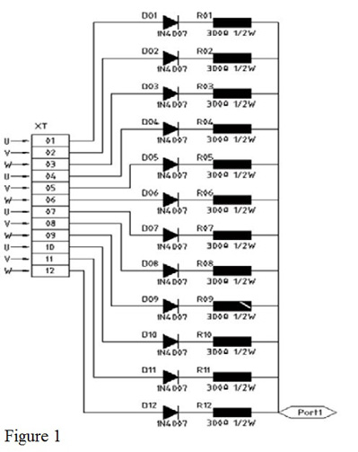
Take a corridor public electricity equipartition as an example. In order to ensure the normal operation of the circuit, multi-channel power is utilized to provide electricity to power module that is AC-DC module with the parameters "Uin=AC85~264V". IN4007 rectification LED that is series with 300Ω1/2W carbon resistor is utilized by multi-channel input for isolation. Figure 1 is the circuit diagram of this product.

Theoretically, it is a perfect idea while there are serious problems in the actual use. Without spike voltage considered, in the normal situations, the voltage between multi-channel power can reach AC400V and the withstand voltage of IN4007 can reach 1000V. The right components are picked up, right? But the fact is that the short cut blast often happens because of the withstand voltage problem, leading to the scrap of the whole product. Of course, it can't be denied that the low quality of components and the aging of LEDs also contribute to the problem. But even if high-quality LEDs or LEDs with higher withstand voltage are installed instead of previous ones, the problem still stands there.
Considering the quality problems of early fatigue within warranty and the existence of throughput yield (TPY), it is nearly impossible for components to reach 100% TPY. As to this circuit, 24 rectification LEDs are required in this advanced circuit with the scrap rate range from 2.4% to 7.2%. PCBs with such a quality are never capable of fully realizing customers' needs. As a matter of fact, here is an easy to use way to handle this problem. As long as one more IN4007 is placed series in each loop, this problem will be easily dealt with. Because at this time, the circuit voltage is reduced by 0.7V, it has no effect to output. Only a little increase of cost brings about the double withstand voltage values and a decrease of error occurrence to 0.5%.
Solutions to Electromagnetic Interference by the Frequent Operation of Midget Relay
The electromagnetic interference brought by the midget relays on PCBs since arc discharge will be produced when they are cutting high current. The interference not only influences the normal operation of CPU, leading to frequent reset, but makes decoders and drivers produce wrong signals and instructions that result in the error of component implementation as well. All these influences will cause defective goods and accidents. In order to solve this problem, two aspects can be considered: increasing the anti-interference capability of CPU and reducing the interference source.
1. Increase the anti-interference capability of CPU. A CPU with high anti-interference capability must be installed. The selection of CPUs also need experiments and test. For example, 90C52RC SCM is an ideal selection. This type of CPU features 20KV anti-static capability and 4KV anti-fast pulse and electromagnetic capability.
2. Reduce the interference source
• Relay-driven amplifiers are capable of effectively reducing the interference generated by back electromotive force when coil is in an outage.
• RC absorption circuit is connected parallel between relay contacts so that noise interference can be rapidly absorbed.
• Circuit boards are copper clad. Copper clad is greatly helpful in reducing the relay interference.
• Relays must be carefully selected. Relays with the same specification always have selections of different coil power. The basic principle is that the larger the coil power is, the more quickly the relay contact on-off actions become, the shorter the time of arc discharge between contacts is, the shorter the electromagnetic interference time becomes.
The Improvement of Pad Off
Neither disassembly nor soldering can be avoided when PCBs are under maintenance. The aging PCBs or PCBs with too small pads always witness the pad off and soldering layer off on plate hole wall when components are disassembled from PCBs.
1. As to the pin pad off, the nearby pad on the same route can be connected to it with a short line that can be selected according to the distance and the amount of current it can hold. For the short distance, the trimmed discarded pins or pin header can be used for soldering; for the long distance, copper wires with outside insulating layer can be used for connection in order to avoid the short cut caused by the connection between lines and pins of other components. When pad off problem always takes place in this place, it can be verified that the PCB design here is so irrational that the design of pads must be optimized. Pads can be designed into long-round or water drop shape within the usable space and short and thick copper clad lines can be added to increase its absorption capacity towards PCB material.
2. As to the soldering layer off on plate hole wall, the reason lies in the small size of the plate hole. When components are disassembled from PCBs, comes along with the soldering layer of plate hole wall. So it's suggested that the size of pad hole should be 0.3 to 0.5mm larger than that of pins in the process of design. When soldering tin layer on the pad hole wall has been fallen off, this method can be tried. Pins of new components should be installed before tin coating with the soldering tin layer a little thicker. Next is the pin soldering. The soldering tin layer on the pin is capable of soldering the pads on PCBs easily.
Replacement of Vulnerable Components
As long as the electronic components are used, some parts become vulnerable and need to be changed or replaced. The usual method of maintaining these components is through soldering that leads to much time consumption, strongly influencing the work efficiency. It is suggested that bases are added to vulnerable components or connections can be made through plugs or insert rows. This method helps engineers save a lot of time and effort.
PCB design and optimization is a complicated process, requiring both a design blueprint and trivial details. Optimizing each detail leads to time consumption and cost decrease in PCB manufacturing process.
Discuss Your PCB Project with PCBCart, And Get Your PCB Design File Checked for FREE!
When choosing PCBCart as your PCB manufacturer, we will carry out a FREE DFM Check on your pcb file before production. If any possible PCB problems detected, we will be in touch to solve them together! This procudure helps guarantee the final circuit boards work exactly as you designed! Wanna to take advantage of our DFM Check? Click the following button to quote for your PCB prices and submit the order. We will get back to you shortly!
Get FR PCB Fabrication Quote - No MOQ Required!
Helpful resources:
• Ultimate Printed Circuit Board Design Guide
• PCBCart Provides Full Feature PCB Fabrication Service
• Except for PCB Fabrication, PCBCart Also Offers Advanced Turnkey PCB Assembly Service
• PCB Design File Requirements for Quick PCB Assembly Quote and Production


