Electronics are an integral part of our daily lives. Everything from our smart phones to our cars includes electronic components. At the heart of these electronics is the printed circuit board, also known as a PCB.
Most people recognize printed circuit boards when they see them. These are the small green chips covered in lines and copper parts you'll find at the heart of gutted electronic devices. Made with fiberglass, copper lines and other metal parts, these boards are held together with epoxy and insulated with a solder mask. This solder mask is where that characteristic green color comes from.
However, have you ever observed those boards with components solidly stuck on? Never regard them as just decorations of a PCB board. An advanced circuit board won't be able to give its functionality until components are mounted on it. A PCB with components mounted on is called an assembled PCB and the manufacturing process is called PCB assembly or PCBA for short. The copper lines on bare board, called traces, electrically link connectors and components to each other. They run signals between these features, allowing the circuit board to function in a specifically designed way. These functions range from the simple to the complex, and yet the size of PCBs can be smaller than a thumbnail.
So how exactly are these devices made? The PCB assembly process is a simple one, consisting of several automated and manual steps. With each step of the process, a board manufacturer has both manual and automated options from which to choose. To help you better understand the PCBA process from start to finish, we've explained each step in detail below.
PCB Design Basics
The PCBA process always starts out with the most basic unit of the PCB: the base, which consists of several layers, and each one plays a significant role in the functionality of the final PCB. These alternating layers include:
• Substrate: This is the base material of a PCB. It gives the PCB its rigidity.
• Copper: A thin layer of conductive copper foil is added to each functional side of the PCB — on one side if it's a single-sided PCB, and on both sides if it's a double-sided PCB. This is the layer of copper traces.
• Solder mask: On top of the copper layer is the solder mask, which gives each PCB its characteristic green color. It insulates copper traces from unintentionally contacting other conductive materials, which could result in a short. The solder, in other words, keeps everything in its place. Holes in the solder mask are where solder is applied to attach components to the board. Solder mask is a vital step for smooth manufacturing of PCBA since it stops soldering from taking place on unwanted parts with shorts avoided.
• Silkscreen: A white silkscreen is the final layer on a PCB board. This layer adds labels to the PCB in the form of characters and symbols. This helps indicate the function of each component on the board.
These materials and components remain largely the same across all PCBs, with the exception of the substrate. The substrate material of a PCB changes according to the specific qualities — such as cost and bendability — each designer is looking for in their finished product.
The three primary PCB types include:

• Rigid PCB: The most common type of PCB base is a rigid one that accounts for majority of PCBAs. The solid core of a rigid PCB gives the board rigidity and thickness. These inflexible PCB bases consist of a few different materials. The most common is fiberglass, otherwise designated as "FR4". Less expensive PCBs are made with materials like epoxies or phenolics, though these are less durable than FR4.
• Flexible PCB: Flexible PCBs offer a bit more pliability than their more rigid counterparts. The material of these PCBs tends to be a bendable, high-temperature plastic like Kapton.
• Metal Core PCB: These boards are yet another alternative to the typical FR4 board. Made with a metal core, these boards tend to spread heat more efficiently than others. This helps dissipate heat and protect more heat-sensitive board components.

There are two types of mounting technologies are prevailing in the modern PCBA industry:
Surface Mount Technology: Sensitive components, some very small, such as resistors or diodes are placed automatically onto the surface of board. This is called SMD assembly, for surface mount device. Surface mount technology can be applied on small size components and integrated circuits (ICs). For example, PCBCart is capable of mounting package with min. size 01005, which is even smaller than the size of a pencil point.
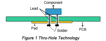
Thru-Hole Technology: works well on components with leads or wires that have to be mounted on board by plugging them through holes on board. The extra lead part has to be soldered on the other side of the board. This technology is applied on PCB assemblies containing large components such as capacitors, coils to be assembled.

Due to distinctions between THT and SMT, they have to go through different assembly processes as well. The following article will discuss other material and design considerations beyond the base of the PCB as they apply to the PCB assembly process in relation to THT, SMT and mixed technologies.
Before the Assembly Process
A few preparatory steps have to happen before real PCBA process even begins. This helps PCB manufacturers assess the functionality of a PCB design, and primarily includes a DFM check.
Most companies specializing in PCB assembly need the design file of the PCB to start out, along with any other design notes and specific requirements. This is so the PCB assembly company can check the PCB file for any issues that may affect the PCB's functionality or manufacturability. This is a design for manufacturability check, or DFM check, for short.

The DFM check looks at all the design specifications of a PCB. Specifically, this check looks for any missing, redundant or potentially problematic features. Any of these issues may severely and negatively influence the functionality of the final project. For example, one common PCB design flaw is leaving too little spacing between PCB components. This can result in shorts and other malfunctions.
By identifying potential problems before manufacturing begins, DFM checks can cut manufacturing costs and eliminate unforeseen expenses. This is because these checks cut down on the number of scrapped boards. As part of our commitment to quality at a low cost, DFM checks come standard with every PCBCart project order. PCBCart provides FREE DFM and DFA check with, however, priceless values because Valor DFM/DFA check PCBCart depends on is an automatic system contributing to high speed and accuracies.
Actual PCBA process steps.
Step 1: Solder Paste Stenciling
The first step of PCB assembly is applying a solder paste to the board. This process is like screen-printing a shirt, except instead of a mask, a thin, stainless-steel stencil is placed over the PCB. This allows assemblers to apply solder paste only to certain parts of the would-be PCB. These parts are where components will sit in the finished PCB.

The solder paste itself is a greyish substance consisting of tiny balls of metal, also known as solder. The composition of these tiny metal balls is 96.5% tin, 3% silver and 0.5% copper. The solder paste mixes solder with a flux, which is a chemical designed help the solder melt and bond to a surface. Solder paste appears as a grey paste and must be applied to the board at exactly the right places and in precisely the right amounts.
In a professional PCBA line, a mechanical fixture holds the PCB and solder stencil in place. An applicator then places solder paste on the intended areas in precise amounts. The machine then spreads the paste across the stencil, applying it evenly to every open area. After removing the stencil, the solder paste remains in the intended locations.
Step 2: Pick and Place
After applying the solder paste to the PCB board, the PCBA process moves on to the pick and place machine, a robotic device places surface mount components, or SMDs, on a prepared PCB. SMDs account for most non-connector components on PCBs today. These SMDs are then soldered on to the surface of the board in the next step of PCBA process.
Traditionally, this was a manual process done with a pair of tweezers, in which assemblers had to pick and place components by hand. These days, thankfully, this step is an automated process among PCB manufacturers. This shift occurred largely because machines tend to be more accurate and more consistent than humans. While humans can work quickly, fatigue and eyestrain tends to set in after a few hours working with such small components. Machines work around the clock without such fatigue.

The device starts the pick and place process by picking up a PCB board with a vacuum grip and moving it to the pick and place station. The robot then orients the PCB at the station and begins applying the SMTs to the PCB surface. These components are placed on top of the soldering paste in preprogrammed locations.
Step 3: Reflow Soldering
Once the solder paste and surface mount components are all in place, they need to remain there. This means the solder paste needs to solidify, adhering components to the board. PCB assembly accomplishes this through a process called "reflow".
After the pick and place process concludes, the PCB board is transferred to a conveyor belt. This conveyor belt moves through a large reflow oven, which is somewhat like a commercial pizza oven. This oven consists of a series of heaters which gradually heat the board to temperatures around 250 degrees Celsius, or 480 degrees Fahrenheit. This is hot enough to melt the solder in the solder paste.

Once the solder melts, the PCB continues to move through the oven. It passes through a series of cooler heaters, which allows the melted solder to cool and solidify in a controlled manner. This creates a permanent solder joint to connect the SMDs to the PCB.
Many PCBAs require special consideration during reflow, especially for two-sided PCB Assembly. Two-sided PCB assembly need stenciling and reflowing each side separately. First, the side with fewer and smaller parts is stenciled, placed and reflowed, followed by the other side.
Step 4: Inspection and Quality Control
Once the surface mount components are soldered in place after the reflow process, which doesn't stand for completion of PCBA and the assembled board needs to be tested for functionality. Often, movement during the reflow process will result in poor connection quality or a complete lack of a connection. Shorts are also a common side effect of this movement, as misplaced components can sometimes connect portions of the circuit that should not connect.

Checking for these errors and misalignments can involve one of several different inspection methods. The most common inspection methods include:
• Manual Checks: Despite upcoming development trend of automated and smart manufacturing, manual checks are still relied on in PCB assembly process. For smaller batches, an in-person visual inspection by a designer is an effective method to ensure the quality of a PCB after the reflow process. However, this method becomes increasingly impractical and inaccurate as the number of inspected boards increases. Looking at such small components for more than an hour can lead to optical fatigue, resulting in less accurate inspections.
• Automatic Optical Inspection: Automatic optical inspection is a more appropriate inspection method for larger batches of PCBAs. An automatic optical inspection machine, also known as an AOI machine, uses a series of high-powered cameras to "see" PCBs. These cameras are arranged at different angles to view solder connections. Different quality solder connections reflect light in different ways, allowing the AOI to recognize a lower-quality solder. The AOI does this at a very high speed, allowing it to process a high quantity of PCBs in a relatively short time.
• X-ray Inspection: Yet another method of inspection involves x-rays. This is a less common inspection method — it's used most often for more complex or layered PCBs. The X-ray allows a viewer to see through layers and visualize lower layers to identify any potentially hidden problems.
The fate of a malfunctioning board depends on PCBA company's standards, they will be sent back to be cleared and reworked, or scrapped.
Whether an inspection finds one of these mistakes or not, the next step of the process is to test the part to make sure it does what it's supposed to do. This involves testing the PCB connections for quality. Boards requiring programming or calibration require even more steps to test proper functionality.
Such inspections can occur regularly after the reflow process to identify any potential problems. These regular checks can ensure that errors are found and fixed as soon as possible, which helps both the manufacturer and the designer save time, labor and materials.
Step 5: Through-Hole Component Insertion
Depending on the type of board under PCBA, the board may include a variety of components beyond the usual SMDs. These include plated through-hole components, or PTH components.
A plated through-hole is a hole in the PCB that's plated all the way through the board. PCB components use these holes to pass a signal from one side of the board to the other. In this case, soldering paste won't do any good, as the paste will run straight through the hole without a chance to adhere.
Instead of soldering paste, PTH components require a more specialized kind of soldering method in later PCB assembly process:
• Manual Soldering: Manual through-hole insertion is a straightforward process. Typically, one person at a single station will be tasked with inserting one component into a designated PTH. Once they're finished, the board is transferred to the next station, where another person is working on inserting a different component. The cycle continues for each PTH that needs to be outfitted. This can be a lengthy process, depending on how many PTH components need to be inserted during one cycle of PCBA. Most companies specifically try to avoid designing with PTH components for this very purpose, but PTH components are still common among PCB designs.
• Wave Soldering: Wave soldering is the automated version of manual soldering, but involves a very different process. Once the PTH component is put in place, the board is put on yet another conveyor belt. This time, the conveyor belt runs through a specialized oven where a wave of molten solder washes over the bottom of the board. This solders all of the pins on the bottom of the board at once. This kind of soldering is nearly impossible for double-sided PCBs, as soldering the entire PCB side would render any delicate electronic components useless.
After this soldering process is finished, the PCB can move on to the final inspection, or it can run through the previous steps if the PCB needs additional parts added or another side assembled.
Step 6: Final Inspection and Functional Test
After the soldering step of the PCBA process is finished, a final inspection will test the PCB for its functionality. This inspection is known as a "functional test". The test puts the PCB through its paces, simulating the normal circumstances in which the PCB will operate. Power and simulated signals run through the PCB in this test while testers monitor the PCB's electrical characteristics.

If any of these characteristics, including voltage, current or signal output, show unacceptable fluctuation or hit peaks outside of a predetermined range, the PCB fails the test. The failed PCB can then be recycled or scrapped, depending on the company's standards.
Testing is the final and most important step in PCB assembly process, as it determines the success or failure of the process. This testing is also the reason why regular testing and inspection throughout the assembly process is so important.
After PCBA
Suffice it to say, PCB assembly process can be a filthy one. Soldering paste leaves behind some amount of flux, while human handling can transfer oils and dirt from fingers and clothing to PCB surface. Once all is done, the results can look a little dingy, which is both an aesthetic and a practical issue.
After months of remaining on a PCB, flux residue starts to smell and feel sticky. It also becomes somewhat acidic, which can damage solder joints over time. Additionally, customer satisfaction tends to suffer when shipments of new PCBs are covered in residue and fingerprints. For these reasons, washing the product after finishing all the soldering steps is important.
A stainless-steel, high-pressure washing apparatus using deionized water is the best tool for removing residue from PCBs. Washing PCBs in deionized water poses no threat to the device. This is because it's the ions in regular water that do damage to a circuit, not the water itself. Deionized water, therefore, is harmless to PCBs as they undergo a wash cycle.
After washing, a quick drying cycle with compressed air leaves the finished PCBs ready for packaging and shipment.
Differences between PCBAs: THT Assembly, SMT Assembly and Mixed Technology

Thru-Hole Technology (THT) Assembly Process
As a traditional PCB assembly method, thru-hole mounting process is accomplished through collaboration of manual procedure and automatic procedure.
• Step 1: Components Placement - This step is achieved manually by professional engineering staff. Engineers need to quickly, yet precisely place components on corresponding positions based on client's PCB design files. Component placement must conform to regulations and operation standards of thru-hole mounting process to guarantee high quality end products. For example, they have to clarify polarity and orientation of components, to stop operating component from affecting ambient components, to make completed component placement compatible with corresponding standards and to wear anti-static wristbands when dealing with static-sensitive components like ICs.
• Step 2: Inspection & Rectification - Once component placement is completed, the board is then placed in a matching transport frame where board with components plugged in will be automatically inspected so as to determine whether components are accurately placed. If issues concerning component placement are observed, it's easy to get them rectified immediately as well. After all, this takes place prior to soldering in PCBA process.
• Step 3: Wave Soldering - Now the THT components should be accurately soldered onto circuit board. In the wave soldering system, the board moves slowly over a wave of liquid solder at high temperature, approximately 500°F. Afterwards, all leads or wires connections can be successfully obtained so that thru-hole components are firmly attached to the board.
Surface Mount Technology (SMT) Assembly Process
Compared with thru-hole mounting process, surface mounting process stands out in terms of manufacturing efficiency because it features a totally automatic mounting PCB assembly process from solder paste printing, pick and place and reflow soldering.
• Step 1: Solder Paste Printing - Solder paste is applied on the board through a solder paste printer. A template ensures that solder paste can be accurately left on correct places where components will be mounted, which is also called stencil or solder screen. Because quality of solder paste printing is directly associated with quality of soldering, PCBA manufacturers focusing on high quality products usually carry out inspections after solder paste printing through a solder paste inspector. This inspection guarantees printing has achieved regulations and standards. If defects are found on solder paste printing, printing has to be reworked or solder paste will be washed off prior to second printing.
• Step 2: Components Mounting - After coming out of solder paste printer, PCB will be auto-sent to pick-and-place machine where components or ICs will be mounted on corresponding pads in the effect of tension of solder paste. Components are mounted on PCB board through component reels in the machine. Similar to film reels, component reels carrying components rotate to provide parts to the machine, which will quickly stick parts to the board.
• Step 3: Reflow Soldering - After every component is placed, the board passes through a 23-foot-long furnace. A temperature of 500°F causes the solder paste to liquefy. Now the SMD components are bound firmly to the board.
Mixed Technology
With the development of modern science and technology, electronic products are becoming increasingly complex, driving complicated, integrated and smaller size PCB boards. It is almost impossible for PCBAs containing only one type of component taking part in.
Most boards carry Thru-hole components and SMD components, which requires collaboration of thru-hole technology and surface mount technology. Nevertheless, soldering is a complicated process that tends to be affected by too many elements. Thus, it becomes extraordinarily significant to better arrange the sequence of thru-hole tech and surface mount technology.
PCBA with application of mixed technologies should be carried out in the following situations:
• Single Side Mixed Assembly: Single side mixed assembly conforms to the following manufacturing procedure: Note: Hand soldering can be applied instead of wave soldering when only a small quantity of THT components is required in this type of assembly.

• One Side SMT & One Side THT: Note - This type of PCB assembly procedure is not recommended since adhesives will burden the total cost of PCBA and possibly lead to some soldering issues.

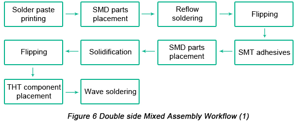
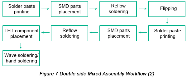
• Double Side Mixed Assembly: In terms of double side mixed assembly methods, there are two alternatives: PCBA with application of adhesives and PCBA without. The application of adhesives increases the overall cost of PCB assembly. Moreover, during this PCBA process, heating has to be carried out for three times, which tends to lead to low efficiency.


Based on the comparison between mixed assembly procedures introduced above, it can be concluded that hand soldering works well for PCB assembly that requires with many components on both sides among which SMD components are more than THT components. Therefore, confronted with the situation when a small number of THT components are needed, it is wave soldering that is suggested.
PCB assembly has to go through such a complicated and technical process that numerous elements have to be taken into careful consideration and a little modification may cause huge change on cost and product quality. Descriptions concerning PCB assembly process in this article just center on typical PCBA procedures and technologies. Practical manufacturing process is largely determined and influenced by design files and specific requirement of customers. As a result, how to evaluate a reliable PCB assembler becomes a crucial question customers have to think it over prior to their PCBA order.
PCBA Professionals
PCBCart is the premier PCB solutions provider. We can cover your PCB requirements from parts sourcing to electronic assembly. We'll help you with each step of the way and provide you with comprehensive expertise and quality assurance.

When you choose us as your cooperative PCBA company, you're choosing to partner with a service that delivers the best. Our PCB assembly services meet the highest quality benchmarks and follow IPC Class 3, RoHS and ISO 9001:2008-certificitation standards . Additionally, we can handle any kind of PCB, whether it's double-sided or single-sided, an SMT, through-hole or mixed-assembly project. Whatever you want done, we can make it happen!
We'll keep in contact with you constantly from the beginning of the project all the way through to the finish line and keep you in the loop from fabrication to assembly. This can help you save money and stress with lower PCB costs, shorter wait time and higher-quality products. We want to save you time and energy so you can focus on your PCB designs — not worry about the minutiae of the manufacturing process.
Start an Instant Quote for PCB Assembly
To learn more about Electronic Assembly, and what PCBCart can do for your next PCB project, take a look at following pages:
• A Comprehensive Introduction of PCBA
• How to Evaluate PCB Assembly Houses?
• PCBCart Offers Advanced Turnkey PCB Assembly Service without MOQ Requirement
• Design for Manufacture and Assembly of PCBs and General Rules It Conforms to
• Design PCBs to Better Take Advantage of PCBCart's PCB Assembly Capabilities
• Instruction on Getting Precise PCB Assembly Prices


