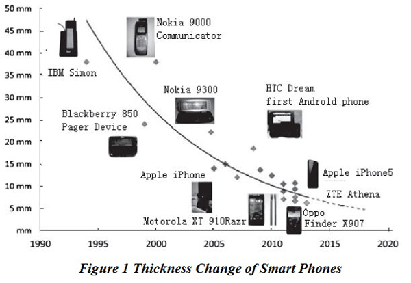
Do you still remember IBM Simon? It is the "father" of smart phones. It came out around 1995 and was the most creative electronic product at that time. However, it didn't look like what a smart phone looks at present and it weighed 510g with a thickness of 38mm. Can you believe it? It's totally impossible for you to put it in your pocket.
With the improvement of functions and people's aesthetic attitude towards cell phones, smart phones have experienced a series of changes in terms of size and figure. Figure 1 indicates the thickness change of smart phones in the past years.

Besides smart phones, manufacturers of pads and desktops are all striving for miniaturization. All these size reductions depend on the design and use of High Density Interconnect PCBs (HDI PCBs). If you just think HDI PCB is only the Herbalife for smart devices, you are definitely wrong. The function of HDI technology aims to make smart devices lighter, smaller, thinner and more reliable.
HDI PCBs refer to the print circuit boards with high density, fine lines, small drill diameter and super thinness. This kind of PCB enjoys fast development since its occurrence based on the protruding advantages:
1. HDI technology can help reduce PCB cost;
2. HDI technology increases the lines density;
3. HDI technology is good for the use of advanced packaging;
4. HDI technology has better electrical performance and signal validity;
5. HDI technology has better reliability;
6. HDI technology is better at heat dissipation;
7. HDI technology is capable of improving RFI (radio frequency interference) / EMI (electromagnetic interference) / ESD (electro-static discharge);
8. HDI technology increases design efficiency;
Material
Some new requirements are brought to HDI PCB material including better size stability, antistatic mobility and non-adhesive. The typical material of HDI PCB is RCC (resin coated copper). There're three types of RCC, namely Polyimide metalized film, Pure polyimide film, Cast polyimide film.
The advantages of RCC include: small thickness, light weight, excellent flexibility and flammability, compatibility with characteristic impedance and excellent size stability. In the process of HDI multi-layer PCBs, taking place of the role of traditional bonding sheet and copper foil as insulating medium and conducting layer, RCC can be suppressed with chip through traditional suppression technology. Then non-mechanical drilling method is used such as laser so that micro-via interconnect can be formed.
The occurrence and development of RCC push PCB products from SMT (surface mount technology) to CSP (chip scale package), from mechanical drilling to laser drilling, and promote the development and progress of PCB micro-via, all of which results in RCC's leading material of HDI PCBs.
In the practical PCB manufacturing process, as for the selection of RCC, ordinarily there is FR-4 standard Tg 140C, FR-4 high Tg 170C and FR-4 and Rogers combined lamination, which are now mostly used. With the development of HDI technology, more requirements must be met by the HDI PCB material, so the main trend of HDI PCB material should be with:
1. The development and application of flex material with no adhesive used;
2. Small thickness of dielectric layer with small deviation;
3. The development of LPIC;
4. Increasingly small dielectric constant;
5. Increasingly small dielectric loss;
6. High soldering stability;
7. Strict compatibility with CTE (coefficient of thermal expansion);
Technology
The difficulties of HDI PCB fabrication lie in micro-via fabrication, via metallization and fine lines.
1. Micro-via fabrication
Micro-via fabrication has always been the core problem in HDI PCB manufacturing. There are two main drilling methods:
1). As for ordinary via drilling, mechanical drilling is always the best choice for its high efficiency and low cost. With the development of mechanical processing capacity, its application in micro-via has been on the way as well.
2). There are two types of laser drilling: photothermal ablation and photochemistry ablation. The former refers to the process during which the operated material is heated to be melted after absorbing laser with high energy and is evaporated off with via formed. The latter refers to the result caused by high-energy photons in UV zone and with laser length more than 400nm.
There are three types of laser systems applied for flex and rigid boards, namely Excimer laser, UV laser drilling, CO2 laser. Laser technology is not only applied in drilling, but in cut and formation as well. Even some manufacturers fabricate HDI by laser. Although laser drilling devices are costly, they have higher accuracy, stable craft and mature technology. The advantages of laser technology make it the most commonly used method in terms of blind/buried via manufacturing. Nowadays, among HDI micro-vias, 99% are obtained by laser drilling.
2. Via metallization
The biggest difficulty for via metallization is it is difficult for plating to reach uniform. As for the deep-hole plating technology for micro-via, besides the usage of plating solution with high dispersing power, via plating solution on plating devices should be upgraded in time that can be accomplished by either strong mechanical stirring or vibration, ultrasonic stirring, horizontal spraying. Also, the humidity of via wall must be increased before plating.
Besides the improvement of the craft, methods of via metallization for HDI see improvement as well with the main technologies: chemical plating additive technology, direct plating technology and so on.
3. Fine lines
The implementations of fine lines include traditional image transfer and laser direct imaging. Traditional image transfer has the same process with the ordinary chemical etching to form lines.
As for laser direct imaging, photographic film isn't needed while images are formed directly on photosensory membrane through lasers. UV wave light is used to operate so that liquid anti-corrosion solution is capable of meeting demands of high resolution and simple operation. Photographic film isn't needed so as to avoid bad influence caused by film defects and CAD/CAM can be connected to it directly so that manufacturing period is shortened to make it suitable for the production of limited quantities and multiple kinds.
PCBCart is capable of manufacturing HDI PCB fabrication with micro-via, via metallization and fine lines. Want to know how much will your HDI PCB production cost? Fee free to submit a quote request on this page with detailed description of your PCB requirements. We will give your HDI PCB price bery quickly.


