KiCad is an open-source software tool for the creation of electronic schematic diagrams and PCB artwork. Beneath its singular surface, KiCad incorporates an elegant ensemble of the following stand-alone software tools:
|
Program Name
|
Description
|
File Extension
|
|
KiCAD
|
Project manager
|
*.pro
|
|
Eschema
|
Schematic editor (both schematic and
component)
|
*.sch, *.lib, *.net
|
|
CvPcb
|
Footprint selector
|
*.net
|
|
Pcbnew
|
Circuit board editor
|
*.kicad_pcb
|
|
Gerb View
|
Gerber viewer
|
All the usual Gerber
|
|
Bitmap2component
|
Convert bitmap images to components
or footprints
|
*.lib, *.kicad_mod,
*.kicad_wks
|
|
PCB Calculator
|
Calculator for components, track width,
electrical spacing, color codes, and more
|
None
|
|
Pl Editor
|
Page layout editor
|
*.kicad_wks
|
KiCad can be considered mature enough to be used for the successful development and maintenance of complex electronic boards. It does not present any board-size limitation and it can easily handle up to 32 copper layers, up to 14 technical layers and up to 4 auxiliary layers. KiCad can create all the files necessary for building printed boards, Gerber files for photo-plotters, drilling files, component location files and a lot more. Being open source (GPL licensed), it represents the ideal tool for projects oriented towards the creation of electronic hardware with an open-source flavour.
1. First run KiCad on your computer. You can enter the main window of the KiCad project manager. From here you have access to eight stand-alone software tools: Eeschema, Schematic Library Editor, Pcbnew, PCB Footprint Editor, GerbView, Bitmap2Component, PCB Calculator and Pl Editor
2. Create a new project: Click File > New Project. Name the project file tutorial1. The project file will automatically take the extension ".pro". KiCad prompts to create a dedicated directory, and click Yes to confirm. All your project files will be saved here.
3. Let's begin by creating a schematic. Start the schematic editor Eeschema  . It is the first button from the left.
4. Click on the Page Settings icon  on the top toolbar. Set the Page Size as A4 and enter the Title as Tutorial1. You will see that more information can be entered here if necessary. Click OK. This information will populate the schematic sheet at the bottom right corner. Use the mouse wheel to zoom in. Save the whole schematic project: File > Save Schematic Project.
5. We will now place our first component. Click on the Place Component icon  in the right toolbar.
6. Click on the middle of your schematic sheet. A Choose Component window will appear on the screen. We're going to place a resistor. Search / filter on the R of Resistor. You may notice the device heading above the Resistor. This device heading is the name of the library where the component is located, which is quite a generic and useful library.
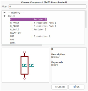
7. Double click on it. This will close the Choose Component window. Place the component in the schematic sheet by clicking where you want it to be.
8. Click on the magnifier icon to zoom in on the component. Alternatively, use the mouse wheel to zoom in and zoom out. Press the wheel (central) mouse button to pan horizontally and vertically.
9. Hover the mouse over the component R and press the "r" key, the component should rotate. You don't need to click on the component to rotate it.
10. Right click in the middle of the component and select Edit Component > Value. You can achieve the same result by hovering over the component and pressing the "v" key. Alternatively, the "e" key will take you to the more general Edit window. Notice how the right-click menu below shows shortcut keys for all available actions.
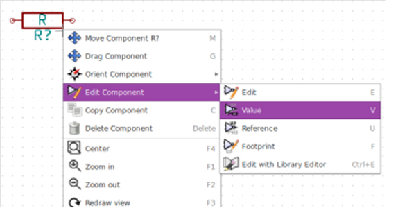
11. The Component value window will appear. Replace the current value R with 1 k. Click OK.
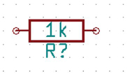
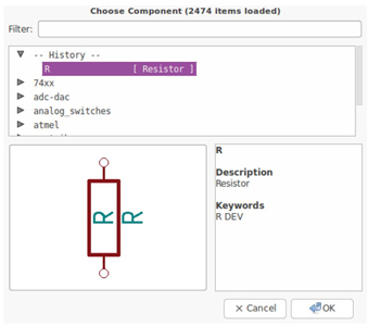
12. To place another resistor, simply click where you want the resistor to appear. The Component Selection window will appear again.
13. The resistor you previously chose is now in your history list, appearing as R. Click OK and place the component.
14. In case you make a mistake and want to delete a component, right click on the component and click Delete Component . This will remove the component from the schematic. Alternatively, you can hover over the component you want to delete and press the "del" key.
15. You can also duplicate a component already on your schematic sheet by hovering over it and pressing the "c" key. Click where you want to place the new duplicated component.
16. Right click on the second resistor. Select Drag Component. Reposition the component and left click to drop.
17. Change the grid size. You have probably noticed that on the schematic sheet all components are snapped onto a large pitch grid. You can easily change the size of the grid by Right-Click > Grid select. In general, it is recommended to use a grid of 50.0 mils for the schematic sheet.
18. We are going to add a component from a library that isn't configured in the default project. In the menu, choose Preferences > Component Libraries and click the Add button for Component library files. Then, you can place power and ground symbols, add pins, make connections using labels with the similar steps as above until electronic schematics is completed.
19. We will now check our schematic for errors. Click on the Perform electrical rules check icon  on the top toolbar. Click on the Run button. A report informing you of any errors or warnings such as disconnected wires is generated. You should have 0 Errors and 0 Warnings. In case of errors or warnings, a small green arrow will appear on the schematic in the position where the error or the warning is located. Check Create ERC file report and press the Run button again to receive more information about the errors.
20. To create a Bill Of Materials (BOM), go to the Eeschema schematic editor and click on the Bill of materials icon  on the top toolbar. By default there is no plugin active. You add one, by clicking on Add Plugin button. Select the *.xsl file you want to use, in this case, we select bom2csv.xsl. Now press Generate. The file (same name as your project) is located in your project folder. Open the *.csv file with LibreOffice Calc or Excel. An import window will appear, press OK.
1. From the KiCad project manager, click on the Pcbnew icon  . The Pcbnew window will open. If you get an error message saying that a *.kicad_pcb file does not exist and asks if you want to create it, just click Yes.
2. Begin by entering some schematic information. Click on the Page settings icon  on the top toolbar. Set paper size as A4 and title as Tutorial1.
3. It is good to start by setting the clearance and the minimum track width to those required by your PCB manufacturer. Generally, you can set the clearance to 0.25 and the minimum track width to 0.25. Click on the Design Rules > Design Rules menu. If it does not show already, click Net Classes Editor tab. Change the Clearance field at the top of the window to 0.25 and the Track Width field to 0.25 as shown below. Measurements are in mm.
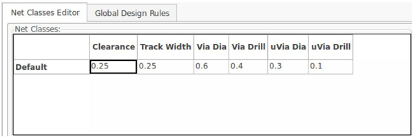
4. Click on the Global Design Rules tab and set Min track width to 0.25'. Click OK to commit your changes and close the Design Rules Editor window.
5. Now we will import the netlist file. Click on the Read Netlist icon  on the top toolbar. Click on the Browse Netlist Files button, select tutorial.net in the File selection dialogue, and click on Read Current Netlist. Then click the Close button.
6. All components are connected via a thin group of wires called ratsnest. Make sure that the Hide board ratsnest button  is pressed. In this way you can see the ratsnest linking all components.
7. You can move each component by hovering over it and pressing the "g" key. Click where you want to place them. Move all components around until you minimize the number of wire crossovers. Then you can make modifications here until you get an ideal PCB layout.
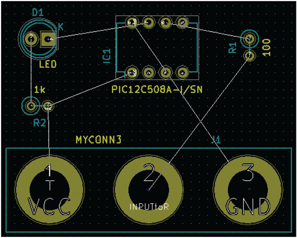
Once your custom circuit design is complete, you can generate Gerber files for each layer and send them to manufacturer for PCB production.
1. From KiCad, open the Pcbnew software tool and load your board file by clicking on the icon  .
.
2. Click on File > Plot. Select Gerber as the Plot Format and select the folder in which to put all Gerber files. Proceed by clicking on the Plot button.
All operations mentioned in this passage are only a part of KiCad overall functions. More detailed will be discovered in your practice.


 . It is the first button from the left.
 on the top toolbar. Set the Page Size as A4 and enter the Title as Tutorial1. You will see that more information can be entered here if necessary. Click
  in the right toolbar.


 on the top toolbar. Click on the
  on the top toolbar. By default there is no plugin active. You add one, by clicking on
  . The Pcbnew window will open. If you get an error message saying that a *.kicad_pcb file does not exist and asks if you want to create it, just click
  on the top toolbar. Set paper size as A4 and title as Tutorial1.

 on the top toolbar. Click on the
  is pressed. In this way you can see the ratsnest linking all components.

 .
.


