As a company serving for more than two decades in PCB industry, PCBCart is fully aware of the significance of time cost and efficiency for our customers. To minimize time intervals from design files to final products, we've summarized a full list containing confirmation items that'll be implemented by our technical engineers. Sufficient preparations definitely help ensure you a smooth and rapid PCB order.
Prior to sending your PCB design files to us, it's necessary for you to check the following items one by one. NOTE: a summary list of table will be provided at the end of this article for engineers with little time to check images and details.
• PCB Design Software Version
PCB design software features different versions that naturally generate different PCB design files holding distinctions between each other in some aspects. To cut your time and ensure the accuracy of your design files, we suggest you tell us your software version in Notes when you submitting the order. Naturally, the OPTIMAL selection is to provide Gerber files.
• Holes
a. Hole Plating
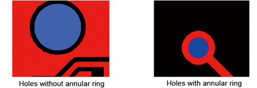
For single-layer PCBs, all the holes should be unplated. For circuit boards with over 2 layers, holes without annular ring in the file should be unplated whereas those with annular ring in the file should be plated.
b. Circles as Holes
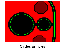
Circles in the mechanical layer or outline layer without copper and have no corresponding holes in the Excellon file will normally be ignored. If you want them to be drilled as holes, please make a note in your PCB design file.
c. Overlapped Holes
There are two types of overlapped holes: 1). When a small hole is inside a bigger hole, they are called totally overlapped holes. The small one should be removed as it is unnecessary when the big one is drilled. 2). When a small hole is crossed with a bigger hole, they are called partially overlapped holes that should be drilled according to the file design.

d. Slot Holes
Two holes in the same pad need to be plated, which is classified into two possibilities: 1). When it comes to two holes in the same copper pad with clearance, spacing of at least 20mil should be left between those holes. Moreover, the two holes should be separately drilled as is indicated in the left image below. 2). When it comes to two slot holes with no clearance between them, they should be shaped as an oval once they are drilled, as is indicated in the right image below.

NOTE: when it comes to holes designed at graphic layer, special mark should be used to highlight them and size, angle and depth should be clarified.
• PCB Mark Design
PCB marks should be appropriately designed and design rules can be learnt from article Design Requirement of SMT PCBs Part Four: Mark.
• V-cut Design
V-cut depth should be reasonably designed. Normally it's one third of the board thickness. Mechanical line should be drawn on PCB design file to indicate where to carry out V-cut.
• Copper Annular Ring
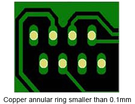
Size of copper annular ring can be figured out by a simple calculation of the diameter of the copper pad minus the diameter of the hole size divided by two. The minimum size of copper annular ring should be 6mil with copper thickness at least 1oz, otherwise it will be broken after completion. The image below is an example in which the annular ring on the left and right of these holes will be broken after completion.
• Spacing between Copper/Trace/Pad and Board Edge
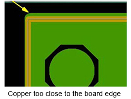
For boards whose edge goes through milling, the spacing should be at least 0.2mm while for boards whose edge goes through v-cut, the spacing should be at least 0.4mm. The image below demonstrates a situation in which the spacing between copper and board edge is out of the safe range. This design may result in the copper being exposed on the edge of the board.
• Spacing between Hole/Via Edge and Board Edge
For routing outline, safe spacing between hole edge and board edge is 0.4mm while safe spacing between via edge and board edge is 0.2mm.
For v-scoring/v-grooving outline, safe spacing between hole to board edge is 0.8mm while safe distance between via and board edge is 0.4mm.
• Via Hole Design
Via holes must NOT be designed between bare copper area and non-bare copper area.
• Spacing between Via Hole Edge and Pad Edge
Spacing between via hole edge and pad edge should be at least 8mil and covered with solder mask.
• Aperture of Mask/Resin Plugged Via
Aperture of mask/resin plugged via should be 16mil at most.
• Aperture of Micro Via
Aperture of micro via should be less than 5mil.
• Gold Finger Bevel
For gold finger requiring to be designed to be a bevel, the ordinary angle is 35°, 45° or 60°.
• Spacing between Positioning Hole Edge and Pad Edge
Spacing between positioning hole edge and pad edge should be at least 0.65mm.
• Board Layer
A board must contain pad layer, silkscreen layer and routing layer.
• Pads
Multiple pads can never be combined together and they should stay independent from each other.
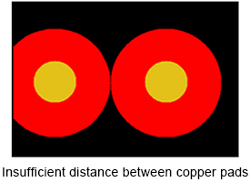
Spacing between copper pads should be at least 5mil. The image below indicates an example of a design in which spacing between the two copper pads is too small, possibly leading to a short circuit once finished.
• Spacing between Copper Grids
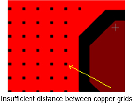
Spacing between copper grids should be 10mil*10mil. Take the image below for example, the spacing between copper grids is smaller than demanded. As such, the grids could not be made out properly.
• Flower Copper Pad in Inner Layers
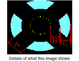
As is indicated in the image below, the best flower pad with clearance A should be 12mil and 10mil for both B and C.
• Legend
a. Legend on Copper Layer
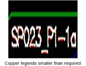
Width of legend lines on copper layer should be at least 10mil and width and height of legends should be at least 28mil*40mil. Spacing between legends should be at least 6mil. If copper legends are smaller than required, the finished legends will be fuzzy, as is indicated in the image below.
b. Legend on Solder Mask
Width of legend lines on solder mask should be at least 8mil and the width and height of legends should be at least 20mil*30mil. Similar with silkscreen/legend on copper layer, if solder mask legends are smaller than required, the finished legends will be fuzzy as well.
c. Legend on Silkscreen Layer
Width of legend lines on silkscreen layer should be at least 5mil and width and height of legends should be at least 20mil*30mil. Spacing between legends should be at least 4mil. If silkscreen legends are smaller than required, the finished legends will be fuzzy.
d. Silkscreen Legends Cover on Copper Pads
Silkscreen legends covers on copper pads will affect PCB soldering. It's suggested that circuit board should be designed such that silkscreen legends are positioned away from copper pads to avoid overlapping.
e. Silkscreen Legends on Thick Copper
Thick copper refers to anything in excess of 4oz. If the same silkscreen legend covers both copper and substrate material, silkscreen legends will be broken and become unclear due to the “step” caused by thick copper. We recommend that silkscreen legends are located either on copper or on substrate material but not across them.
• Solder Mask
a. Size of Solder Mask Resist Openings
Solder mask resist openings should typically be 2mil to 3mil larger than copper pads and should be the same shape as copper pads that should have solder mask openings on both top and bottom sides.
b. Shifting of Solder Mask
Solder mask resist opening should NOT be shifted from copper pads.
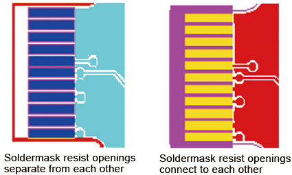
c. Solder Mask Resist Opening for IC Pads or Gold Finger Pads
There are two circumstances available: 1). Openings are separated from each other for IC pads and there'll be a solder mask resist oil bridge between IC pads after circuit board manufacturing is completed, as is indicated in the left image below. 2). Openings are connected to each other for IC pads and there'll be no solder mask resist oil bridge between IC pads once PCB manufacturing is completed.
• Drilling Holes
Position, size and number of drilling holes should be appropriately designed. If you have some special designs, you can make our engineers informed by taking some notes while making your order.
• Others
When it comes to flex-rigid PCB design, circuits should be respectively designed for flexible part and rigid part or a schematic diagram of lamination can be generated to clarify rigid and flexible layers.


