As lines on PCB (Printed Circuit Board) ready to be used for SMT (Surface Mount Technology) assembly become finer, components miniaturized and SMDs (Surface Mount Devices) high-density assembled, visual inspection is far, far away from being sufficient to be compatible with SMT assembly quality inspection demands. As a result, AOI (Automated Optical Inspection) becomes increasingly commonly used in SMT assembly as a key method to inspect the performance of soldering joints formed in SMT assembly procedure. In addition, AOI has been applied in wider application fields and its inspection technology becomes gradually advanced and optimal. Right now, AOI system is moving towards intelligentization as an inspection mode used in SMT assembly.
Working Logic of AOI Technology
Although AOI technology has been used in different forms in SMT assembly, they share the same working logic, that is, optical methods are used to capture the figure of inspected target and inspections, analysis and judgment can be made in certain way. The commonly-used inspection, analysis and judgment method in AOI system includes DRC (Design Rule Check) method and CAD (Computer-Aided Design) data comparison method.
•DRC Method
DRC method is used to inspect design pattern based on some given rules. For example, PCB circuit pattern is inspected in accordance with the rule that all lines should rely on solder joints as terminals, all lines share the same width and spacing should be equivalent or larger than a regulated value. DRC method is capable of guaranteeing the validity of the pattern from algorithm. In addition, DRC method features some advantages, including easy setup, high-speed processing, and small volume of programming and small data storage. Therefore, AOI system mostly depends on DRC method.
The obvious disadvantage of DRC lies in its weakness in determining boundary capability and boundary position should be determined by designing particular method.
•CAD Data Comparison Method
CAD data comparison method is used to compare the digital image patterns stored in AOI system with the practical image patterns that are captured to summarize inspection result. The accuracy of this method depends on inspection accuracy, definition and all inspection procedures and can be obtained high. However, disadvantages of this method include high volume of captured data and high requirement on data real-time processing.
As DRC method and CAD data comparison method are compared, the latter enjoys more merits.
Inspection Functions of AOI Technology
AOI technology can be used to implement inspections on PCB bare boards, solder paste printing, components and solder joints.
Bare PCB inspection and solder joint inspection usually depend on independent AOI instrument and the inspections are not made in real time. Solder paste inspection and component inspection usually depend on the AOI instrument matching solder paste printer and chip mounter and their inspections are made in real time. For example, currently advanced solder paste printer is capable of carrying out real-time inspections on printing thickness and printing edge collapse through the matched AOI system.
AOI items for bare PCBs cover disconnection, wiretapping, scratches, pinhole, line spacing and tracing, edge roughness and mass-area defects. AOI items for solder joints cover lead arrangement and bending, missing components, misplacement, components placement direction, component number, solder joint quality etc. As AOI system finds out unqualified components, signals will be usually sent to operators who will be able to replace them with qualified components and stop errors from making disasters in volume.
Structure of Typical AOI System
•AOI System for Bare PCBs
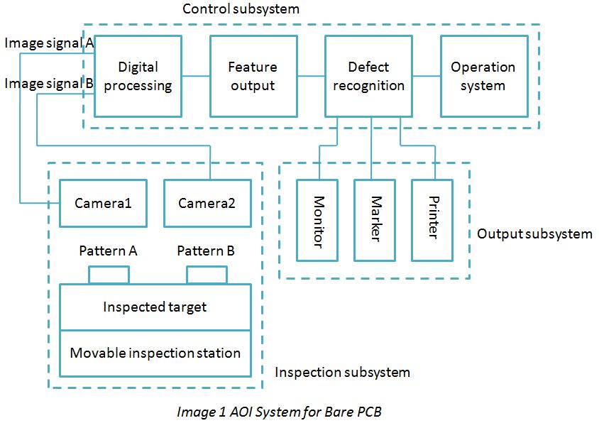
Image 1 below demonstrates the AOI system for bare PCBs.
Based on AOI design rules, this system adds comparison function and prepares two cameras. Inspection subsystem uses 1D image sensor to capture images of traces on PCBs and the image signals will be sent to control subsystem after being corrected and high-speed A/D transformed. The control subsystem then makes judgment on defects and scanning will be made through moving inspection stations along a direct line from front to back so that image sensors can get 2D image output signals. Marks will be made on PCB defects in ink in real time and defects can be magnified and shown on monitor so visual inspection can be used to check.
System operation can be implemented in the form of dialogue on monitor and output subsystem consists of digital image monitor, real image monitor, printer and synchroscope. The system allows digital colored image and real images to be respectively displayed on monitors with output printed out. In addition, figures of image signals and digital clip level can be observed through synchroscope. The inspection speed of this type of system can be as high as a few meters per minute, minimum resolution can be a micrometer level and the minimum line width and space between lines can be a couple of micrometers.
•AOI System for Solder Joints
The working logic of AOI system for solder joints is that optical cameras are used to capture 3D images of solder joints that will be compared with standard solder joint images after data processing so that defect category and positions can be judged and clarified.
•AOI System for Solder Paste Printing
AOI system for solder paste printing consists of camera and optical fiber x-y system. Camera is installed on x-y desktop with optical fiber moving in the direction of x-y and the complete image of PCB can be obtained.
In the process of solder paste printing, solder paste is pressed into openings on stencil by scraping blade and the ideal effect should be that solder paste thickness is equivalent to that of stencil. When stencil is moved away from PCB, some changes will occur to solder paste edge.
Solder paste inspection system depends on annular optical fiber and annular reflector to make slant light to shine on solder paste with camera capturing images from the straight direct of annular optical fiber so that the edge part of solder paste can be measured and solder paste thickness can be figured out. This inspection makes judgement by transforming shapes into optical changes. Even in ordinary printing situation, some promontories will be generated in edge part to make some strong reflections.
Getting AOI Service from PCBCart
PCBCart provides AOI service to customers ordering either PCB and PCBA from PCBCart. What’s better, it’s totally FREE! Plus, customers can expect X-ray inspection service from PCBCart to further guarantee quality and performance of your products.