Theoretically, PCB (Printed Circuit Board) current carrying capacity is determined by cross-sectional area of trace and temperature rise. Furthermore, cross-sectional area of trace is directly proportional to trace width and copper thickness. Well, here comes a question: does this rule also apply to the relationship between current carrying capacity and trace cross-sectional area, that is, is trace carrying capacity directly proportional to its cross-sectional area? Under the same temperature rise that is 10°C, a 10mil-trace with 1oz copper weight is capable of withstanding current of 1amp at most and we rest assured that a 50mil-trace is capable of withstanding current larger than 1amp. Then how exactly is the maximum current it is able to hold, 5amps based on a simple multiple calculation? It's actually far more complicated than that. According to MIL-STD-275, we are told that the maximum current a 50mil-trace can stand is 2.6amps.
|
Temp rise
|
10°C
|
20°C
|
30°C
|
|
Copper
|
0.5oz
|
1.0oz
|
2.0oz
|
0.5oz
|
1.0oz
|
2.0oz
|
0.5oz
|
1.0oz
|
2.0oz
|
|
Trace width (inch)
|
Max. current amps
|
|
0.01
|
0.5
|
1.0
|
1.4
|
0.6
|
1.2
|
1.6
|
0.7
|
1.5
|
2.2
|
|
0.015
|
0.7
|
1.2
|
1.6
|
0.8
|
1.3
|
2.4
|
1.0
|
1.6
|
3.0
|
|
0.02
|
0.7
|
1.3
|
2.1
|
1.0
|
1.7
|
3.0
|
1.2
|
2.4
|
3.6
|
|
0.025
|
0.9
|
1.7
|
2.5
|
1.2
|
2.2
|
3.3
|
1.5
|
2.8
|
4.0
|
|
0.03
|
1.1
|
1.9
|
3.0
|
1.4
|
2.5
|
4.0
|
1.7
|
3.2
|
5.0
|
|
0.05
|
1.5
|
2.6
|
4.0
|
2.0
|
3.6
|
6.0
|
2.6
|
4.4
|
7.3
|
|
0.075
|
2.0
|
3.5
|
5.7
|
2.8
|
4.5
|
7.8
|
3.5
|
6.0
|
10.0
|
|
0.1
|
2.6
|
4.2
|
6.9
|
3.5
|
6.0
|
9.9
|
4.3
|
7.5
|
12.5
|
|
0.2
|
4.2
|
7.0
|
11.5
|
6.0
|
10.0
|
11.0
|
7.5
|
13.0
|
20.5
|
|
0.25
|
5.0
|
8.3
|
12.3
|
7.2
|
12.3
|
20.0
|
9.0
|
15.0
|
24.0
|
Nevertheless, the table above has been gradually replaced by IPC-2221 Generic Standard on Printed Board Design as a reference based on which a printed circuit board is accurately designed.
Copper Thickness Measurement Unit
Prior to genuine discussion, it's necessary to wiki a unit applied for copper thickness, ounce (oz). It is generally accepted as a unit for weight measurement but in circuit board design, it has been employed for copper thickness measurement. When it comes to the conversion on copper thickness by ounce, some rules should be kept in mind. Because specifications of copper are measured by copper weight per square feet, 1oz that is usually mentioned actually refers to the fact that each square feet of this copper is 1oz in terms of weight. Under such cases, the thicker copper is, the more it weighs since copper weight is directly proportional to its thickness. As a result, copper thickness can be represented by weight unit, ounce. Furthermore, ounce can be also transferred into units of millimeter or mil. Some ordinary conversions are listed below:
0.5oz = 0.0007inch = 0.7mils = 0.018mm
1.0oz = 0.0014inch = 1.4mils = 0.035mm
2.0oz = 0.0034inch = 2.8mils = 0.070mm
Relationship between PCB Copper Foil Cross-Sectional Area and Maximum Current Carrying Capacity and Temperature Rise
Based on the explanation of Section 6.2 in IPC-2221, that is, Conductive Material Requirements, current carrying capacity can be further classified into two types: internal conductors and external conductors. Maximum current carrying capacity of internal conductors is defined as half of that of external conductors. Table 6-4 in IPC-2221 demonstrates the relationship between copper foil cross-sectional area, temperature rise and maximum current carrying capacity among external conductors and internal conductors.
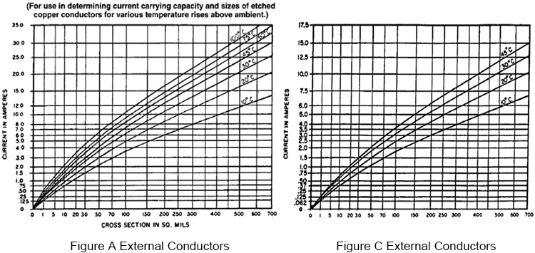
Moreover, a simplified formula has been summarized based on the tables above: I = KΔT0.44A0.75
In this formula, K is a correction factor. It is equivalent to 0.024 in terms of internal conductors and 0.048 for external conductors. ΔT is the Max. temperature difference, indicating the temperature difference between heating copper and ambient temperature with its unit to be degrees Celsius (°C). A refers to cross-sectional area of copper trace with its unit to be square mil (mil²). I refers to current carrying capacity with its unit to be ampere (Amp).
Owing to the development of electronic technology, some online trace width calculators are available for circuit board designers. It's such a handy tool that as soon as demanded current and copper weight are filled, corresponding trace width of internal conductors and external conductors will be provided. PCB Trace Width Calculator and ANSI IPC-2221A PCB Trace Width Calculator belong to the tools introduced just now.
Elements Determining Maximum Current Carrying Capacity
Although a simple formula can be directly employed to calculate maximum current carrying capacity, practical cases are not that simple and direct. That's because apart from cross-sectional area and temperature rise, trace current carrying capacity also depends on other elements such as number of components, pad and vias.
For traces with many pads distributed, the tinning trace will perform an extremely higher capacity than ordinary traces. It's not a rare condition in which engineers meet circuit boards on which some trace between pads is burned down as a large current is flowing through. The reason for such tragedy lies in too much solder paste on components or pins leads to an increased cross-sectional area while no modification occurs to trace between pads. As a result, as soon as power starts or order modification is implemented on trace, it's possible to cause a super large transient surge or even burning down of a trace between pads.
One of the solutions to this issue lies in trace width increasing. When a trace isn't allowed to be widened, solder mask can be applied on traces that tend to be burned down and solder paste should be printed in SMT (Surface Mount Technology) procedure. After reflow soldering, trace width will rise so that current carrying capacity will go up as well.
In one word, though PCB trace current carrying capacity can be obtained by table provided by IPC or a formula, they are only applied for straight trace calculation. However, dust or contaminant pollution has to be taken into careful consideration in real printed circuit fabrication or assembly because pollution will possibly lead partial traces broken. Thus, when we are designing maximum current carrying capacity in either way, a security factor has to be added to prohibit overloading issue from taking place.
Moreover, special attention has to be paid to turning traces. If an acute angle takes place in a trace, non-smooth transfer will possibly be caused, which perhaps leads to little influence on small current or trace with high width. But when it comes to low current carrying capacity, issues may take place.
PCB current carrying capacity is something to be considered while designing effective and reliable circuit boards. However, theoretical calculations themselves might not suffice to make effective decisions when implemented in practical scenarios. That is why using industry standards like IPC-2221 is necessary so that your PCB performs as designed under actual operating conditions.
To ensure your PCB designs tackle these challenges well, consider partnering with PCBCart. We specialize in providing quality PCB manufacturing services that align with today's standards for assurance and performance. Order a free quote today and get a solid foundation for your next project!
Get Your PCB Quote Now
Helpful Resources
• Thick Copper PCB Fabrication Service
• PCB Material Selection Guide in PCBCart
• Guide on Getting PCB Fabrication Price within Seconds
• High Quality Standard PCB with 20+ Years of Experience | PCBCart


