Recent years have been witnessing improvement in electronic information technology and increasingly higher demands from people on their applications of electronic products. Complex structure and multiple functions of electronic products lead printed circuit boards (PCBs) to move towards new directions. On one hand, increasingly more integrated components in electronic products and miniaturization of overall size make circuit boards be of high density, high accuracy and high integration, which arousing a transition from simply multilayer PCBs to HDI PCBs. On the other hand, electronic products call for high-speed, low loss, low delay and high-fidelity (HiFi) signal transmissions and have to be compatible with high-consumption environment for high powers, requiring PCBs to be involved with a high-frequency and high-dissipation thermal design and high-quality signals transmission.
To cater to the demands and market trend, technologies concerning high frequency, high thermal dissipation and high density interconnect designs have been receiving the most attention in modern PCB industry and will be a leading development trend in the future.
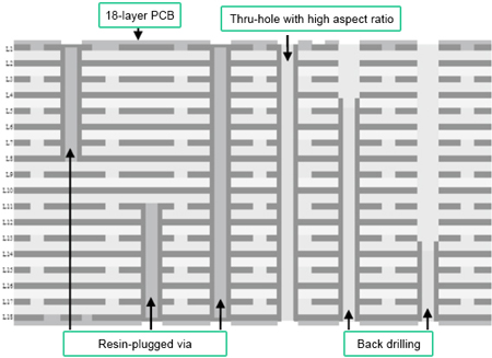
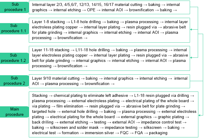
In this article, we take an 18-layer PCB (a multilayer circuit board containing participation of numerous advanced designs including multiple back drilling, high aspect ratio resin-plugged via and high-thermal dissipation via) with high-frequency material as a study example, to detail technologies applied in the process of this circuit board fabrication, such as resin-plugged via, stacking up, high-density drilling and back drilling.
Substrate Material
High frequency, signals with a frequency band to be at least 300MHz (equivalent to wavelength no more than 1m), can be further classified into medium frequency (MF) and very high frequency (VHF) according to different wavelengths. Electromagnetic waves whose wavelength is at least 1GHz are usually referred to microwaves. As PCB's majority functions are determined by substrate material, substrate material featured by high frequency will be applied in high-speed and high-frequency PCBs. High-frequency substrate material has to meet the following demands:
a. Dielectric constant (Dk) should be small and stable (generally speaking, the smaller, the better). Based on principle which signal transmission rate is inversely proportional to square root of material dielectric constant, high dielectric constant tends to cause delaying signal transmission.
b. When it comes to signal transmission quality, dielectric loss (Df) should be small as well. The smaller Dk is, the smaller signal loss will be.
c. Copper foil should have a surface with low roughness to avoid impedance control mismatching and signal loss caused by skin effect.
d. Substrate material for high-frequency and high-speed PCBs should feature low hydroscopicity. Dielectric constant of water is 70 and this number will be increased when substrate absorbs more moisture. Thus, modification of impedance control will lead to badly-performed signal transmission.
e. Copper foil should conform to relatively high peel strength that mustn't be compromised just due to low surface roughness.
f. Substrate material should also perform excellently in terms of size stability, heat resistance, chemical resistance, impact strength and manufacturability.
In conclusion, much care has to be taken with above aspects and items considered when deciding suitable substrate material for high-frequency and high-speed multilayer PCBs. For example, the following table details comparison between substrate materials provided by different distributors.
|
Item
|
Material A
|
Material B
|
Material C
|
Material D
|
|
Dk
|
2.1-2.5
|
2.4-2.7
|
3.5-3.8
|
4.0-4.5
|
|
Df
|
0.0009-0.0017
|
0.0007-0.001
|
0.009-0.013
|
0.018-0.022
|
|
Tg
|
25°C
|
210°C
|
185°C-220°C
|
120°C
|
|
Ion-Migration Resistance
|
A>B>C>D
|
|
Ion-Migration Resistance
|
A>B>C>D
|
|
Moisture Resistance
|
A>C>B>D
|
|
Manufacturability
|
D>C>B>A
|
|
Cost
|
A>B>C>D
|
Based on integrated comparison in terms of substrate material dielectric constant, dielectric loss, Tg, ion-migration resistance, moisture resistance, manufacturability and cost, we use Material C for this type of high-frequency and high-speed multilayer printed circuit board.
• Resin-plugged via manufacturing
a. Issue description
Resin-plugged via manufacturing have long been plagued engineers and manufacturers in PCB industry, especially for PCB products with high density and integrity. Taking advantage of resin-plugged via, people have been expecting to defeat defects that can't be solved through oil-plugged via or stacking resin-plugged via. Nevertheless, high resin-plugged via quality can never be obtained until lots of difficulties are met due to attributes of resin-plugged via itself and structural features of printed circuit boards.
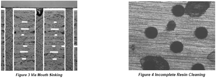
The high-frequency and high-speed multilayer printed circuit board introduced in this article is an 18-layer 2.65mm board. The maximum layer count conforming to requirement of resin-plugged via is 18 layers and vias are designed into multiple groups with different via diameters: 0.25mm and 0.5mm and the highest aspect ratio can be 11:1. As a PCB containing high aspect ratio and multiple via designs demands ordinary plugging via technique and vias of different sizes need different levels of pressure, on one hand, some issues tend to be caused including via mouth sinking, internal cavity, bubbles and oil overflowing, as is shown in Figure 3. On the other hand, incomplete resin cleaning tends to be caused later. Once incomplete resin cleaning takes place, it's suggested that grinding be carried out for a second time for one or two times. Too many times of grinding shrinks yield and also leads to quality issues such as deformed board, insufficient copper thickness and broken via mouth.

b. Solutions
Prior to resin plugging, circuit board has to be dried to guarantee non-existence of moisture inside via, which aims to stop separation between via copper and resin due to moisture inside via. Before being used, resin has to be stirred and go through defoaming in order to eliminate internal bubbles inside resin and to reduce resin viscosity. Under such circumstance, opportunities will be created for resin-plugged vias with a high aspect ratio. When vacuum plugging machines are being applied for resin plugging, small vias with high aspect ratio have to be fully plugged to stop bubbles from being generated so that quality of resin-plugged vias can be ensured.
With rein-plugged vias completed, pre-solidification has to be carried out on resin based on stage baking by abrasive belt prior to grinding. Specific baking parameters are summarized into the following table.
|
Temperature
|
Baking time
|
|
80°C
|
20min
|
|
100°C
|
20min
|
|
130°C
|
20min
|
|
150°C
|
30min
|
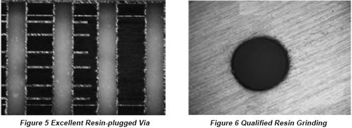
With the items listed in the table above rigorously followed, some quality issues can be prohibited including separation between resin and copper and cracks on resin. Furthermore, beneficial conditions can be created for resin grinding owing to incomplete solidification of resin with some issues avoided such as deformed board and insufficient copper thickness. Figure 5 indicates an excellent resin-plugged via with smooth via mouth and without bubbles or cavity inside via while Figure 6 demonstrates qualified resin grinding.

• Stacking-up
a. Issue description
Laminated boards are such a catastrophe that is usually witnessed among PCB products. Along with application of lead-free soldering technology, laminated boards take place more frequently especially on high density interconnect (HDI) boards.
This type of circuit board used in this article is an 18-layer HDI PCB throughout two-time stacking. With application of high-frequency board material, multiple groups of resin-plugged buried via have been designed through Layer 1 to Layer 18 and they are densely distributed with spacing to be 0.26mm between vias. As a result, weak binding force will be formed between vias. Moreover, binding force between resin and prepreg sheet is so weak that lamination will be caused in the area where resin-plugged buried vias are densely placed after high-temperature soldering.
b. Solutions
Lots of elements contribute to the occurrence of lamination in the area where resin-plugged buried vias are densely placed. Solutions derive from aspects including material selection, PCB fabrication, manufacturing procedure etc.
The first element to consider lies in compatibility between plugging oil, substrate material and Tg and CTE (coefficient of thermal expansion). When a relatively large distinction takes place between them, plugging oil and substrate material will reach their own Tg temperature intervals and different levels of expansion will be caused under the same heating time and temperature rise speed. Therefore, the solution to that lies in optimal determination of resin for plugging based on substrate material Tg and CTE.
Owing to limited binding force between plugging resin and prepreg, inefficient adhesive in prepreg of buried via area and incomplete leaving resin grinding, subsequent lamination will still be led as a result of bad binding force between layers. In order to improve resin plugging technique, pre-solidification should be carried out prior to grinding to make resin fully grinded prior to total solidification so that resin will be stopped leaving. Prepreg stacking has to be designed again and prepreg containing a high content of adhesive should be applied in resin-plugged density area in order to ensure sufficient stacking flow adhesive and heat resistance of end products.
When dense via area and board margin receive bad drilling and milling, lamination can be also caused as a result of mechanical stress. Totally new drilling blade and resin aluminum cover should be applied in dense via area. Drilling and stacking count should be reduced as well and bit bouncing should be applied with baking board used after drilling. Mechanical stress should be reduced and mechanical drilling should be improved to reduce its influence on board via structure. Count of tool vias should be shrinked and lifespan of milling blade and stacking number should be controlled.
Printed circuit boards tend to absorb moisture in the process of fabrication and absorbed moisture will be evaporated in later high temperature and expanded under copper, leading to huge pressure. Moreover, binding force between resin and prepreg and copper layer is so weak that peeling tends to be caused and so does lamination. Therefore, during the producing procedure, moisture absorption should be rigorously monitored and controlled.
• Dense heat dissipation hole manufacturing
a. Issue description
Heat dissipation can never be neglected since high-frequency and high-speed multilayer PCB is involved with requirement of high frequency, high density, high accuracy and high integrity. On one hand, compared with ordinary multilayer PCBs, high-density, high-accuracy and high-integrity design contains so many components assembled with a high density. On the other hand, high-frequency, high-speed and high-function design of HDI PCBs calls for larger power. Small space and large power will definitely bring challenges to heat dissipation of final products and strongly compromising PCB reliability. Based on structural features and high-frequency and high-speed performance, high-density heat dissipation hole design should be relied on. Heat dissipation holes, equivalent to high-density metalized holes, play a role of a thin copper conduit that goes through along PCB thickness direction, making heat of components flow towards the back side of PCB and fast transmitted to other dissipation layers.
High-density heat dissipation holes feature a relatively simple theory but it's not that simple to focus on their quality insurance in PCB manufacturing procedure. For example, when a high-frequency and high-speed multilayer PCB whose margin is designed to be a high-density heat dissipation hole area with more than 1000 holes whose diameter is 0.50mm and spacing is 1.2mm, ordinary drilling method doesn't work because drilling cuttings won't be eliminated in time while heat produced by drill fails to be dissipated, which will definitely lead to melting drillings that will be attached to hole wall. Once they cool down, a large amount of glue refuse will be formed, greatly compromising quality of hole walls. What's worse, holes may be blocked when glue refuse potentially exceeds. This type of blocked holes can hardly be cleaned up and is a potential danger for PCB products.
b. Solutions
Ordinary drill has to be replaced by a totally new type of drill for holes drilling to avoid issues like rough hole wall and concentrating heat caused by insufficient drill length, drill abrasion and bad level of cuttings elimination. Vacuuming and suction pressure should be modified from 0.014MPa to 0.02MPa, increasing the amount of drilling cuttings. Resin cover is applied to replace ordinary aluminum cover, capable of absorbing heat generated in the process of drilling, reducing drill temperature, making drill become lubricating, shrink drilling contaminants and improving drilling quality.
Another solution that works lies in bit bouncing technology for high-density small holes manufacturing with drill heat dissipation time and cuttings elimination time lengthened and issues alleviated such as cutting blocking, concentrating heat and rough hole wall.
• Back drilling production
a. Issue description
Transmission return circuit of high-speed and high-frequency signals mainly relies on copper tracing and graphics printed on board. When copper is punctured by a thru-hole, return circuit will be compromised with signals fallen into a mess.
For example, when signals are transmitted from top layer to some internal layer, an extra stub will be created to implement electric connection. High-speed signals will be divided into two parts: one part will be reflected back when it enters bottom layer and the other part enters internal circuit along normal route. Differentiations in terms of phases of two types of signals lead to the existence of resonance due to interference caused at some frequency point. Resonance evidently enlarges insertion loss that is ambient to resonance frequency, greatly compromising signal transmission. The longer stub is, the larger capacity will be so that a lower resonance frequency will be created, which will substantially lower transmission quality of signals. Three approaches are available to solve this problem: substrate material thickness reduction, high-speed signals placement at bottom layer or application of back drilling referring to a process during which a drill whose diameter is larger than that of hole is used to eliminate metalized hole wall, that is, stub will be eliminated as well.
Up to now, back drilling is a relatively low-cost high-frequency and high-speed printed circuit boards manufacturing method capable of meeting their demands. However, in actual manufacturing, some quality issues will possibly take place such as internal hole metal, hole blocking and cut drilling due to limitations of back drilling structure.
The ordinary procedure pre-process→board plating→external graphics→graphic plating→external etching→back drilling→post-process tends to call for issues like internal via burr and copper wires. In the process of hole drilling, because electro-copper on hole wall features relatively weaker binding force compared with RA copper on substrate material with copper attached to its surface, hole copper tends to peel in the process of hole drilling, leading to via burr and copper wires. Furthermore, copper thickness inside a hole is generally required to be at least 20μm. Since copper foil features excellent malleability, it's difficult to be cut down when hole drilling. Plus, occurrence of hole burr also derives from unsuitable drilling angle of back drilling or incompatibility of back drilling parameters.
b. Solutions
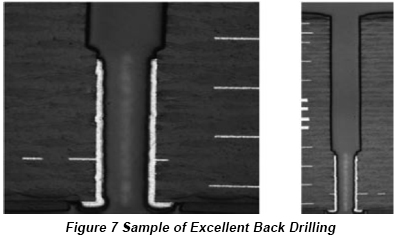
A back drill with a suitable angle should be picked and manufacturing parameters compatible with drilling angle should be found so as to stop burr from taking place inside a hole due to unsuitable angle, insufficient rotating speed and incomplete cutting capacity. Therefore, the following procedure should be applied instead: pre-process→board plating→external graphics→graphic plating→back drilling→external etching→post-process. Once back drilling is arranged prior to external etching and etching solution is depended to eliminate hole burr and copper wires, holes can be prohibited from being blocked. An excellent backing drilling sample is displayed below.
