As a must-have part held by electronic products, Printed Circuit Boards (PCBs) play a key role in implementing functionality of electronic products, which leads to the protruding importance of PCB design because PCB design performance directly determines function and cost of electronic products. Excellent PCB design is able to make electronics products far away from lots of issues so as to ensure products will be smoothly manufactured and be capable of meeting all demands of practical application.
Among all the elements contributing to PCB design, Design for Manufacture (DFM) is definitely an essential one since it links PCB design and PCB manufacturing so that problems will be exposed early and solved in time during the whole life cycle of electronic products. It has been a myth that the complexity of PCB design will be increased as electronic products' manufacturability is taken into consideration during PCB design phase. When it comes to life cycle of electronic product design, DFM cannot only make electronic products smoothly get involved in automatic manufacturing with labor cost saved during manufacturing process, but can effectively shorten manufacturing production to guarantee timely completion of final electronic products.
PCB Manufacturability
Design for Manufacturing is a key element leading to high-efficiency manufacturing, high quality and low cost now that manufacturability and PCB design are combined. PCB manufacturability study features a wide range that can be classified into PCB fabrication and PCB assembly in general.
• PCB Fabrication
As far as PCB fabrication is concerned, the following aspects should be taken into consideration: PCB size, PCB shape, technical rail and fiducial mark. Once those aspects fail to be fully considered during PCB design stage, fabricated PCB boards possibly can't be accepted by automatic chip mounter unless extra processing measures are made. It's even worse that some boards fail to be able to be involved in automatic manufacturing with manual soldering leveraged. As a result, manufacturing period will be prolonged and labor cost will rise as well.
a. PCB Size
Each chip mounter has its own required PCB size that differs from each other in accordance with parameters of each mounter. For example, the maximum PCB size accepted by chip mounter in PCBCart is 500mm*450mm while the minimum PCB size is 30mm*30mm. It doesn't mean we can't deal with PCB board assembly smaller than 30mm*30mm and when smaller size is required, panels can be relied on. Chip mounters never accept PCB boards that are either too large or too small in size when only manual mounting can be depended with labor cost rising and production period out of control. Thus, during PCB design stage, PCB size requirement set by automatic mounting manufacturing has to be fully considered and it must be controlled within a valid range.
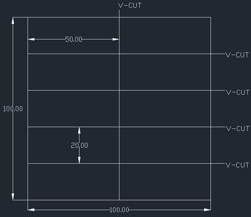
Below image demonstrates a PCB panel design file completed by EDA software. As a 5x2 panel, each square unit is a single board with its size being 50mm*20mm. Connection between each single unit is achieved by V-cut/V-scoring tech. In this image, the whole square displays the final size of panel that is 100mm*100mm. Based on the panel size requirement mentioned above, it can be concluded that the panel size falls into the agreeable range.
Note: if you are interested in ordering PCBs in panel type, please refer to this guide to get PCB panel prices.

b. PCB Shape
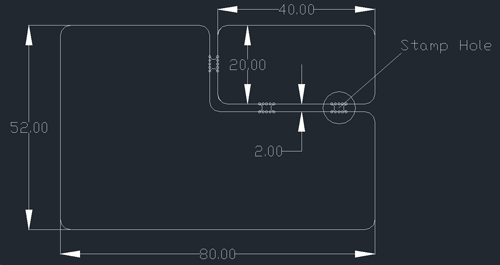
Apart from PCB size, all chip mounters lay requirement in terms of PCB shape as well. Ordinary PCB shape should be a rectangle whose ratio between length and width should be 4:3 or 5:4 that are optimal. When a PCB features an irregular shape, extra measures have to be made before SMT assembly, leading to cost increase. In order to stop that from taking place, PCBs have to be designed to be in ordinary shape during PCB design stage so that SMT requirement can be met. Nevertheless, it can hardly be achieved in practical situations. When some electronic products have to be irregular on shape, stamp holes plus bridge have to be used to make the shape of final PCB have an ordinary shape. After assembly, extra part can be eliminated from PCB, which satisfies both the requirement of automatic mounting and space.
Below image indicates an irregular-shape PCB with processing edge added through EDA software. The whole board size is 80mm*52mm while the square area is the size of practical PCB. The size of upper right corner area is 40mm*20mm, which is processing edge resulting from stamp holes plus bridge.

c. Technical Rail
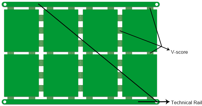
In order to meet demands of automatic manufacturing, technical rail has to be placed on PCBs to fix PCBs.
During PCB design stage, a 5mm-wide technical rail should be left in advance where no components and traces are left. It's ordinary to place technical rail at the shorter side of a PCB but the shorter side can be selected when ratio between length and width is over 80%. Technical rail will be eliminated after assembly as a role of subsidiary production.

d. Fiducial Mark
For PCBs with components mounted on, fiducial marks should be added as common reference points ensuring each assembly equipment to accurately determine component positions. Therefore, fiducial marks are benchmarks of SMT manufacturing, necessary for automatic manufacturing.
Components call for 2 fiducial marks while PCBs call for 3 fiducial marks, which should be placed at PCB board edge and cover all SMT components. Center distance between fiducial mark and board edge should be at least 5mm. For PCB with double sides carried SMT components, fiducial marks should be available on both sides. If components are placed too densely to place fiducial marks on board, they can be placed on technical rail.
• PCB Assembly
PCB assembly, short as PCBA, is actually the process of soldering components on bare PCB boards. In order to meet requirement of automatic manufacturing, PCB assembly sets up some requirement on component package and component layout.
a. Component Package
During PCBA design process, if component package doesn't conform to suitable standards with distance between components too close to each other, automatic mounting won't be carried out.
To obtain optimal package for components, professional EDA design software should be used to be compatible with international component package standards. In PCB design process, bird's-eye view area should never be overlapped with other area and automatic IC mounters will be able to accurately recognize and carry out surface mounting.
b. Component Layout
Component layout is an important task in PCB design because its performance is directly associated with what PCBs will look and complexity level of manufacturing process.
During component layout process, assembly sides for SMD components and THD components should be determined. Here, let's set front side of PCB as component A side while back side as component B side. Component layout should take assembly form into consideration including single-layer single-package assembly, double-layer single-package assembly, single-layer mix-package assembly, Side A mix-package and Side B single-package assembly and Side A THD and Side B SMD assembly. Different assembly calls for different manufacturing processes and technologies. Therefore, as far as component layout is concerned, optimal component layout should be selected to make manufacturing become simple and easy, improving manufacturing efficiency of the whole process.
In addition, component layout orientation, spacing between components, thermal dissipation and component height have to be taken into consideration.
Generally speaking, component orientation should maintain consistent. Component layout conforms to the principle of the shortest tracing distance based on which polarity orientation should be consistent for components with polarity marks and components without polarity marks should be neatly arranged on X or Y axis. Component height should be 4mm at most while component and PCB transmission direction should maintain 90 °.
In order to improve component soldering speed and be convenient for later check, spacing between components should be consistent. Components should be close to each other within the same network while safe distance should be left between different networks according to voltage drop. Silkscreen and pad should never be overlapped, otherwise components won't be mounted.
Thermal dissipation issues should be considered due to PCB practical operating temperature and electrical components thermal properties. Component layout should focus on thermal dissipation while fan or heat sink should be used when necessary. Suitable heat sinks should be selected for power components and thermal-sensitive components should be placed far from those generating heat. High components should be placed behind low components.
There are still more details that should be focused on concerning PCB DFM and experience should be accumulated in practice. For example, high-speed signal PCB design calls for special requirement for impedance, which should be discussed with board manufacturer prior to real manufacturing so as to determine impedance and layer up information. For manufacturing preparation on some PCB boards with small size and dense tracing, manufacturing capabilities on minimum trace width and via diameter should be discussed with PCB manufacturer to guarantee smooth manufacturing of those PCBs.
Get Access to FREE DFM/DFA Check from PCBCart
We've been fully aware of the significance of time and cost for customers. DFM/DFA check prior to real manufacturing is capable of determining whether manufacturing can be smoothly implemented based on your design file. Moreover, this service provided by PCBCart is totally FREE, in spite of which, DFM/DFA check service is priceless since the system we take advantage of is Valor DFM Check, a type of automatic system carrying out accurate manufacturability check at a high speed. Contact us for more information about our FREE DFM/DFA Check. It's definitely worth it!
Just finished a new PCB design and looking for PCB House? Check how much you can save when using our custom PCB fabrication service.
Get an Instant Quote for PCB Fabrication
Request FREE Turnkey PCB Assembly Quote
Helpful Resources:
• PCBCart Manufactures PCBs in Any Irregular Shape – NO Extra Fee Charged
• PCBCart Features Advanced PCB Assembly Service – Multiple Value-added Options
• Components Souring Service from PCBCart – NO Counterfeit Electronic Components
• File Requirements for Efficient and Smooth PCB Manufacturing


