With the development of electronic component package technologies towards miniature, light weight and high performance, it has been a development trend of electronic components to increase component function density and decrease spacing between input terminals and output terminals, which is best displayed by automatic assembly technology featured by SMT (surface mount technology). In order to implement surface mounting of components, the first step is to manufacture corresponding pads on PCB so that structured PCB can be obtained. Then, stencil printing technology is applied to cover solder paste on the surface of PCB pads. Finally, heating is carried out to transform solder paste into liquid that is formed into liquid bridge between pins of components and PCB pad. Under the influence of solder mask on PCB, melting solder paste is limited in the corresponding solder pad area in order to prohibit bridging between solder joints so that automatic assembly of chip on PCB is implemented. According to different package types, circular and rectangular solder pads are majorly selected, that is, BGA (ball grid array) and QFN (quad flat no-lead) package. If you want to know more about BGA, just FOUR steps are sufficient.
QFN Wiki
Compared with other components with different types of packages, QFN package is designed to be directly soldered on PCB or FPC substrate. It is capable of offering better heat dissipation owing to its exposed metal pads at the bottom. Furthermore, QFN package features excellent electric performance since its pins are shorter than those of components with extended package. Therefore, it's of great significance to design QFN pads on PCB so that high reliability and performance of PCB can be maintained and ensured.
Wetting Angle
Because the size of QFN pins and spacing between pins are relatively small, solder joint bridge or pseudo soldering may be caused due to accurate amount of tin paste coating. So, reasonable design on pad size of PCB based on the thickness of stencil (h0) is greatly helpful to the success rate of soldering. Suppose the wetting angle of soldering tin on the solder pad (θa) is 30° and the wetting angle of soldering tin on the solder mask (θr) is 160°. If roughness of pad surface is neglected, wetting angle can be regarded approximately as advancing or receding angle of three-phase line of contact. In accordance with practical soldering craft of QFN components, reasonable control on temperature curves of reflow soldering under an ideal condition with soldering tin fully melted and pad surface wetted is capable of both ensuring soldering efficiency and helping components reach automatic assembly soldering balance. If pad is reasonably designed, the ideal state of soldering joints not only meets the requirement of electrical performance of PCB and mechanical connection, but also avoids the failure of solder joints such as bridging and pseudo soldering. In that light, the state of solder joints has to meet the following formulae:
a. When solder joints inside QFN are completely distributed on PCB pad, θa≤θj(Zu)≤θr, θj(0)=30°, x3(0)=x4(0)=Dx4
b. When tin outside QFN is growing in the side pad,
(1) θj(Zu)=θs3+90°, θ4(0)=30°, θ3(0)=30°,
(2) x3(0)=x4(0)=Dx4(0), x3(Zu)=0.
Pad Design
In this formula, θs3 is equal to θa both of which are the wetting angle of solder tin on the side pad.
In the vertical direction, equation of static equilibrium of bridging liquid is:
PdLy(x3(0)-x4(0)+Lx)+Wz-[T(x3(0)-x4(0)+Lx)(sinθ2(0)+sinθ1(0))+TLy(sinθ3(0)+sinθ4(0))]-ρgV0=0
The pressure intensity at the bottom of solder joints (Pd) is: Pd=[T(x3(0)-x4(0)+Lx)(sinθ2(0)+sinθ1(0))+TLy(sinθ3(0)+sinθ4(0))+ρgV0-Wz]/[Ly(x3(0)-x4(0)+Lx)]
In these formulae, ρ refers to the liquid density of soldering tin; T refers to the surface tension of solder joint liquid; x3(0) and x4(0) refer to the slippage of two ends of liquid solder joints at the bottom solder pad liquid; θ1(0) and θ2(0) refer to contact angles on both sides formed by liquid-gas interface on both sides of solder joints and bottom pad surface while θ3(0) and θ4(0) refer to contact angles on both ends formed by liquid-gas interface on both sides; V0 refers to the volume of solder joint; Wz refers to the applied force of pad at the end of chip and solder joint in the vertical direction.
Under the limit of formula (1) and (2), frame curves of solder joints can make boundary conditions equivalent on the upper end of solder joints to initial conditions based on the effective method of solutions to initial value. Since the solution to initial value is incapable of meeting the requirement that z is equal to 0, it is transformed into an equivalent issue in terms of objective function minimization that is displayed in Equation (3).
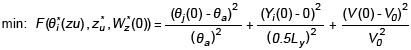
This minimized objective function can be applied to determine the ideal design size of pad Dx4.
Moreover, geometric features of tin wrap angle of PCB pad have to be taken into consideration. In that light, the expansion size of pad should adhere to the about equation below: 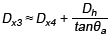
In this equation, Dh refers to the thickness of exposed side pad outside chip. Through the optimization of implicit variables, expected error requirement is met by objective function and the design size of pads inside and outside (Dx4 & Dx3) can be calculated with the need of side value at the lower end met.
This method ensures that a pad suitable for QFN can be well designed in order to reach the high electrical performance of both this component and PCB. Then, with professional and qualified assembly capability, PCBCart is capable of transforming your ideal design into reality.


