PCB successfully added to your shopping cart
Design Requirement of SMT PCBs Part Two: Settings of Pad-Trace Connection, Thru-Holes, Test Point, Solder Mask and Silkscreen
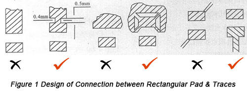
• When pad is connected with the ground with a large area, cross grounding and 45° grounding should be first considered.
• The length of leads drawn from the ground with a large area or power lines should be more than 0.5mm and the width less than 0.4mm.
• The traces connected with rectangular pads should be drawn from the center of the long side of pad with angle generation avoided.

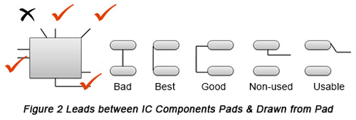
• Design of leads between IC circuit component pads and leads drawn from pad is displayed in Figure 2.

Settings of Thru-Holes
• Settings of Thru-holes (Through holes) in the application of reflow soldering:
a. Generally, the diameter of Thru-holes is at least 0.75mm.
b. Thru-holes can't be placed under other components except components such as SOIC and PLCC.
c. Thru-holes mustn't be directly placed on the pad or its expanded part and corner, which is shown in Figure 3.
d. There should be a fine line with soldermask film between Thru-hole and pad. The length of the fine line should be 0.5mm+ and the width 0.4mm+.

• Thru-holes should be placed in the pad or near the pad in the process of wave soldering, which is helpful for gas release.
Test Point
• Some test points can be placed on PCB, either holes or pads.
• Setting requirement of test points is the same as that of reflow soldering through holes.
• Probe test supports through holes and test points.
In the application of online test, several probe tests should be placed on PCB to support Thru-holes and test points and when they are connected, lines should be drawn from any place of routing. The following aspects should be carefully considered:
a. The minimum spacing must be considered when probes with different diameters are for ATE (automatic test equipment).
b. Thru-holes mustn't be placed on the expansion part of pad, similar with the requirement of reflow soldering through holes.
c. Test points mustn't be determined on soldering points of components.
Soldermask
• PCB should pick up the surface finish of HASL (hot air solder leveling).
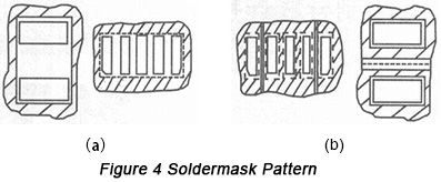
• Size of soldermask pattern should be bigger than pad surrounding edge by 0.05-0.254mm in order to stop soldermask paste polluting pad.
• In the cases of narrow spacing or no leads passing between pads, the soldermask pattern in Figure 4(a) can be followed; in the cases of leads passing between pads, the soldermask pattern in Figure 4(b) can be followed in order to avoid soldering flux bridge connection.

Silkscreen Pattern
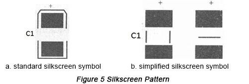
Generally speaking, the silkscreen pattern of components should be marked in the silkscreen layer, including silkscreen symbol, component tag number, polarity and I pin symbol of IC. Simplified symbol can be utilized in the case of high-density and narrow spacing, which is displayed in Figure 5. For special circumstances, component tag number can be omitted.

Got SMT PCB Production Requirements? Reach PCBCart for a free SMT PCB Quote Today!
PCBCart has rich experience in almost all kinds of SMT PCBs manufacturing. We are capable of covering quickturn, production run at any quantity, custom test, system integration and box build all under one roof. Reach us for a free and no-obligation quotation for your SMT PCB project today!
Get an Instant Quote for FR4 PCBs
Helpful Resources
• Elements Ensuring Excellent PCB Pad Design for QFN
• Solder Mask and Its Design Tips
• Design Requirement of SMT PCBs Part One: Bonding Pad Design of Some Ordinary Components
• Design Requirement of SMT PCBs Part Three: Component Layout Design
• Design Requirement of SMT PCBs Part Four: Mark
• Full Feature PCB Manufacturing Service from PCBCart - Multiple Value-added options
• Advanced PCB Assembly Service from PCBCart - Start from 1 piece


