Along with the fast development of very large scale integrated circuits (ICs), electronics assembly demands can never be met by traditional package types and newer packages come into being due to the encouragement of demands in terms of higher integrity, smaller board size and higher I/O count. Among all the newer types of packages mentioned above, BGA (ball grid array) package is a primary type with the widest application fields due to its diversity defeating multiple limitations featured by traditional packages. From the perspective of elements concerning soldering technologies, BGA package is hardly different from traditional packages, QFP (quad flat package) for example. Nevertheless, pins are replaced by solder balls, which can be regarded as a revolution in electronics assembly and brings forward the advent of derivative packages such as CSP (chip scale package). Right now, BGA soldering has still to be implemented with traditional SMT (surface mount technology) applied and BGA soldering can still be carried out in ordinary SMT assembly equipment. This article will discuss some factors affecting the application of BGA assembly technologies including BGA pad design, solder paste printing, mounting alignment accuracy, soldering temperature curves and soldering defects.
Feasibility of BGA Pad Design
BGA packages come in a couple of classifications based on different pitches. Generally speaking, BGA pad design should take CAD tracing feasibility and manufacturability of PCB (printed circuit board) into initial consideration. BGA pad comes in numerous types as well and they can be freely selected when space is allowable with the following types commonly used.
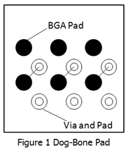
• Dog-bone Pad

Dog-bone pad takes advantage of via to lead trace to other layers so that some limits have been laid to pad size. Due to the existence of vias, some defects tend to be caused during PCB manufacturing process such as soldering bridging due to solder mask falling off. Therefore, pad size has to be designed by rigorously conforming to practical manufacturing level in order to minimize soldering defects generated during BGA soldering and leave some space for BGA rework in the future.
• Vias Distributed Externally to BGA Pads
This type of pad works best for BGA components with low count of I/O. This type of pad design provides convenience to soldering and sets more free space to pad size. Of course, fundamental requirement has to be met in terms of tracing. Thus, it's almost impossible to leverage this type of pad on BGA with higher count of I/O.
• Via-in-pad Pad
Via in pad develops along with the progress of microvia technology in PCB fabrication.
Apart from pad type, solder mask and BGA pad position are directly associated with BGA soldering. Based on different solder mask positions, BGA pads come in two types: SMD (solder mask defined) pad and NSMD (non solder mask defined) pad with respectively functions on BGA soldering. As SMD pad is applied, pad features a large bonded area with pad, which leads to equivalently large bonded area between soldering joints and PCB board. As pad size becomes increasing, however, spacing between adjacent pads becomes small, affecting via pad distribution and tracing capability.
During PCB fabrication procedure, if solder mask deviates along the same direction, BGA pad won't be influenced, which is beneficial to BGA soldering. But this type of pad tends to be broken during solder mask rework at the edge, which is bad for rework effect. Once NSMD pad is used, pad will be relatively small, which is beneficial to via pad distribution and tracing. This type of pad structure, however, results in decreasing bonded area between soldering joints and pad and further reducing soldering joint bonding intensity. In a word, both pads feature their own advantages and disadvantages and corresponding pad can be determined based on technology consideration.
Solder Paste Printing
Solder paste printing plays a key role in determining soldering quality. Solder paste printing is the accurate transformation of solder paste from stencil to pad with stencil, solder paste and printer involved. Precision of solder paste printer should first conform to the demands of BGA assembly. Stencil determines amount of solder paste through its thickness and opening size. The amount of soldering paste called by BGA package is usually determined by 3 aspects:
• Sufficient solder should be used to ensure excellent BGA soldering connections.
• Soldering paste amount should compensate for solder ball co-planarity error (usually 0.1mm) of BGA components.
• When other fine-pitch components are available on circuit board, soldering paste amount should be comprehensively considered to stop more soldering defects from occurring.
Positioning Accuracy
Accurate positions of BGA components on circuit board totally depend on the precision of chip mounters most of which contain specific positioning system which is capable of helping achieving accurate positioning of BGA components. Furthermore, some chip mounters even can inspect BGA solder balls in terms of their co-planarity and recognize some defects such as missing balls, which is extremely helpful for the improvement of BGA soldering reliability.
Furthermore, some other measures can be made to further improve mounting accuracy of BGA components and. For example, local fiducial marks are set at the external part of BGA pads or a couple of fold lines are set as fiducial marks for manual inspection after assembly, both of which have been verified effective in practical manufacturing.
Moreover, BGA components features obvious self-centering effect in the process of soldering due to surface tension of solder so some designers purposely enlarge pads on the four corners in BGA pad design, making self-centering effect more obvious to ensure BGA components be able to self-reset when mounting positions are shifted.
Soldering Temperature Curve and Soldering Defects
Soldering temperature curve directly determines soldering quality. A temperature curve usually includes four phases: preheating phase, soaking phase, reflow phase and cooling phase each of which features different physical/chemical changes. Since temperature curve setting determines the forming process of soldering joints, it features close relationship with the reliability of soldering joints. Due to the particularity of BGA package, it's extremely difficult to generate a satisfying temperature curve. Generally speaking, a BGA component needs three temperatures to be measured: packaging temperature, circuit board surface temperature and the temperature of internal solder joint of BGA.
BGA Inspection and Rework Technologies
Because all BGA solder joints are below packages after soldering, traditional inspection methods such as flying probe test or visual inspection fail to meet practical needs. Up to now, they leading methods that can scan soldering defects of BGA soldering joints is AOI (automated optical inspection) test and AXI (automated X-ray inspection) test.
Based on properties of BGA structure, it's hardly possible to inspect a single soldering joint of BGA component. However, the complete packaging body should be reworked.
Other Factors
Other factors have to be noticed in BGA assembly process such as electrostatic protection and BGA component baking. Usually, BGA components call for special packages with electrostatic protection requirement. During printed circuit board assembly process, rigorous electrostatic protection measures should be made including equipment grounding, staff management and environmental administration.
BGA Assembly at Nice Price
With over 20 years' experience handling PCB Assembly demands from worldwide clients, we have the capabilities to solder almost all kinds of parts into circuit boards, including BGA components. If you have any questions or concerns on PCB Assembly, reach us for knowledge about our PCB solder capabilities and discuss custom PCB population projects. Feel free to click below button to request BGA Assembly Price! It is TOTALLY FREE!
Request for Free PCB Assembly Quotation
Helpful Resources
• A Comprehensive Introduction of BGA
• Top Reasons for Cracks in BGA Soldering
• Solder Ball Issues of BGA Components and How to Avoid Them
• Advanced Turnkey PCB Assembly Service from PCBCart
• How to Get PCB Assembly Prices
• How to Evaluate A PCB Manufacturer or A PCB Assembler


