With the increaseing market demand of HDI (high density interconnect) PCBs, the requirements derived from the market ascend as well. However, traditional process flow has some disadvantages including complexity, high cost, long production cycle and low OTD (on time delivery). In order to decrease the cost, cut down process flow, and shorten production period, blind-hole filled technology develops from previous point-plating blind-hole filling into the present panel-plating blind-hole filling technology. This new type of blind-hole plating technology is capable of both downsizing the production cost and improving the quality of HDI boards. Besides, it even can contribute to the increasing of OTD, providing opportunities for manufacturers to serve more impatient customers.
Different HDI PCB customers have different design requirements, reasonable production process flow must be followed in order to control the cost and ensure the quality. This article will display and discuss some types of process flows of HDI PCBs by the analysis of different types of HDI boards.
Comparison between process flow of point-plating blind-hole filling and that of panel-plating blind-hole filling
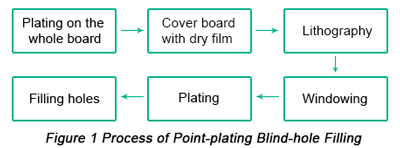
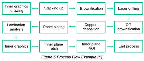
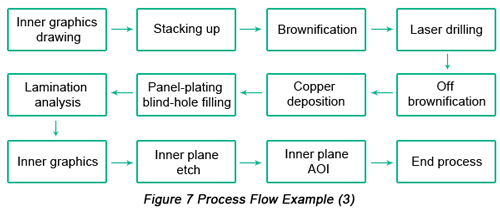
Compared with the process of point-plating blind-hole filling, Panel-plating blind-hole filling follows a much less complex process that blind holes are filled by plating with professional solution. Here's Point-plating blind-hole filling proces:
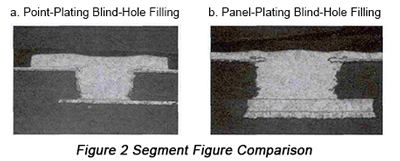
Based on the comparison between segment figures of point-plating blind-hole filling and panel-plating blind-hole filling (Figure 2), it is clear to indicate that copper on the blind hole in the former is much thicker than that in the latter. Extra copper needs to be rubbed down with abrasive belt that has strong pull force for the copper cap, which leads to loose circuit or even scrap.
However, after panel-plating blind-hole filling, copper on the blind hole is so homogeneous that three steps can be omitted including blind-hole plating graphics, film stripping and rubbing down by abrasive belt, which results in shorter process flow and production cost alleviating to avoid scrap caused by abrasive belt.
Technology of Panel-Plating Blind-Hole Filling
The technology of panel-plating blind-hole filling is based on the module of super filling. For copper plating, the electrodeposition rate at the bottom of blind holes is bigger than that at the surface. The distribution of three types of luminescence agents at the bottom and on the surface of blind holes is displayed in Figure 3.
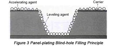
According to the attributes of plating luminescence agent and electrochemical principle, the functioning principles of these luminescence agents are:
-
a. Since leveling agent has positive electricity, it is easily absorbed at the edge of the hole with the most negative electricity and it is dissipated slowly. So the concentration of leveling agent decreases at the bottom of the hole.
-
b. Leveling agent is capable of decreasing polarization, promoting copper deposition, refining grains. It gets together at the density area with low current with a fast dissipation rate so the concentration of accelerating agent gradually increases at the bottom of hole.
-
c. At the edge of the hole with negative electricity with the strongest convection, leveling agent will stop the edge of the hole instead of inhibitor.
Application of Panel-Plating Blind-Hole Filling in Inner Planes of HDI boards
Panel-plating blind-hole filling technology is widely applied in blind holes in HDI boards. However, different types of HDI boards should be paired with different process flows so that suitable process flow must be picked up based on requirements of different customers.
According to the definition of HDI board order, each blind hole manufacturing can be regarded as an order of HDI board. Based on the present technology, the generation of each order in HDI boards needs a stack up, which means that as long as the final stack up is concerned, it is called panel-plating blind-hole filling in inner planes of HDI boards.
• HDI boards with only blind holes in inner planes
HDI boards with only blind holes in inner planes refer to the HDI boards that only have blind holes to connect with other circuits from other planes. The stack up is shown in Figure 4.
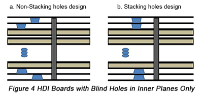
For boards with Design A, blind holes don't need complete filling or leveling up while sufficient plating copper is completed. For boards with Design B, blind holes must be completely filled and leveled up.
When blind holes don't need to be filled or leveled up, the used plating parameters are capable of making blind-hole copper meet corresponding requirements and of ensuring the thickness of inner bronze in the range from 17.1μm to 34.3μm. When blind holes need filling and leveling up, the used plating parameters are capable of both ensuring the completion of filling and leveling up and the thickness of inner bronze beyond 34.3μm. Because blind holes don't need to be filled or leveled up for non-stacking holes so that the process flow of copper elimination isn't needed, when the thickness of inner copper is required to be 34.3μm, blind holes in the inner planes are manufactured into filling holes. Based on the two types of HDI boards mentioned above, the process flow according to different thickness of inner copper is shown as follows:
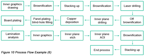
1). Non-stacking blind holes design: with the thickness of inner copper 17.1μm
2). Stacking blind holes design: with the thickness of inner copper 17.1μm
3). When the inner copper thickness reaches 17.1μm, blind holes are filled and leveled up in inner stacking holes design and non-stacking holes design.
Based on the analysis above, when inner blind holes are stacking design, relatively large filling parameters must be used to make blind holes filled and leveled up to ensure the blind holes filled and leveled up. Then copper has to be cut to the required thickness. Therefore, among the three process flows mentioned above, by adjusting holes filling parameters, the thickness of surface copper can be controlled.
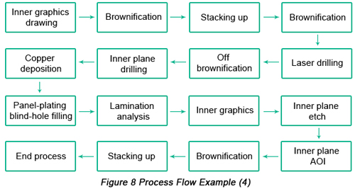
• HDI boards with both blind holes and buried holes in inner planes
This type of HDI boards can be classified as: non-stacking blind and buried holes, stacking blind holes and non-stacking buried holes, stacking buried holes and non-stacking blind holes, stacking blind and buried holes.
For this type of HDI boards, the filling and leveling up extent of blind holes must be considered and the requirement of buried hole copper must be met. Normally, the inner copper thickness of this type is 34.3μm.
Panel-plating blind-hole filling can be only used to produce boards with thickness-to-radius less than 6:1. However, for boards with thickness-to-radius more than 6:1, hole plating process must be implemented in order to meet the corresponding requirement of blind hole copper. Therefore, blind holes and buried holes should be produced respectively, that is, blind holes should be filled and leveled up first and buried holes are then plated by plating holes.
Since blind holes are all produced to make them filled and leveled up, whether blind holes are stacking or not has nothing to do with process flow design. As long as whether buried holes are stacking or non-stacking is determined, it'll be fine. The specific process flows are shown as the following:
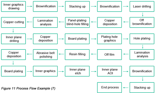
1). The thickness-to-radius of buried hole is less than 6:1 with buried holes non-stacking.
2). The thickness-to-radius of buried hole is less than 6:1 with buried holes stacking.
3). The thickness-to-radius of buried hole is more than 6:1 with buried holes non-stacking.
4). The thickness-to-radius of buried hole is more than 6:1 with buried holes stacking.
Based on the process flows displayed above, stacking-up with gel filling can be used instead of resin filling. PP with large amount of gel is required in the stacking-up with gel filling technology. Although this type of PP is much more expensive than ordinary PP, production processes can be saved and so can the used resin be. Considering the cost, this technology can help decrease the HDI PCBs production cost and time.