With the upcoming development of electronic science and technology, the electronic system composed by IC chip is fast developing toward large scale, miniature and high speed. Simultaneously, a problem comes up as well that the shrinking of the volume of electronic system leads to the enlarging of routing density of circuit while the signal frequency rises constantly and edge turnover time of signal becomes short. When the interconnection delay of signals is larger than signal turnover time by 10%, signal leads on board will display effect of transmission lines, making a series of problems such as signal reflection and crosstalk increasingly protruding. The advent of high-speed problem brings bigger challenge to hardware design and if some designs that are regarded correct from the perspective of logic fail to be unsuitably processed, the whole design will suffer from failure. Therefore, how to solve the problems of high-speed circuits has become one of essential elements determining the success of system.

Principles of Reflection and Its Influence
• Principles of reflection
The direct reason for reflection lies in the incompatibility of impedance of transmission lines that leads to the incomplete absorption of signal energy at the terminal. Reflection issue reflects signal quality of single network, related with physical properties of signal path of single network and returning path. Usually, physical properties of PCB routing has great influence on transmission lines, mainly including routing material, routing width, routing thickness, distance between other routing planes and planes and dielectric constant of adjacent material. When signals are being transmitted along single network, transient impedance change of interconnection lines will be generated. If the interconnection impedance felt by signals keeps unchanged, non-distortion will be maintained. If the interconnection impedance felt by signals keeps changed, distortion will be generated with reflection produced at the change point. The reflection signal will be transmitted back to the emission end of signals and will be reflected back again until it shrinks with the downsizing of energy. Finally, the voltage and current of signals will become stable.
• Calculation of reflection
When signals are transmitted forward along transmission lines, transient impedance will be felt at any time. If the impedance felt by signals is constant, it will be transmitted forward normally. As long as the felt impedance changes, reflection will always be caused no matter what causes. The significant index measuring reflection amount is reflection coefficient indicating the ratio between reflection voltage and original signal voltage. Reflection coefficient can be defined according to formula  .
.
In this formula, Z1 refers to the impedance after change while Z0 the impedance before change. Suppose the characteristic impedance of PCB routing is 50Ω. In the process of transmission, a resistor of 150Ω is encountered and then the reflection coefficient is (150-50)/(150+50)=1/2 (In this circumstance, the influence of parasitic capacitance and inductance isn't considered with resistor as an ideal pure resistor). This result indicates that half of energy of original signal is transmitted back to the source terminal. If the voltage of transmission signals is 5V, reflection voltage is 2.5V.
• Influence of reflection
1). Signal distortion caused by reflection
If a lead isn't terminated correctly, signal pulse from driving end will be reflected at the receiving terminal. When reflected signals are quite strong, stacked waveform will possibly change logic condition that leads to unanticipated effect, causing signal outline distortion. When distortion becomes so obvious, numerous errors will possibly be caused with designed failed. Meanwhile, signals with distortion have more sensitivity towards noise, which will cause design failure as well.
2). Overshooting and undershooting caused by reflection
Overshooting refers to the fact that the first peak value or valley value exceeds voltage. For rising edge, it refers to the fact that the first peak value exceeds the highest voltage while for falling edge, it refers to the fact that the first valley value exceeds the lowest voltage. Exaggerated overshooting will possibly destroy protection diodes, leading to early failure. Undershooting refers to the fact that next valley value or peak value will possibly generate false clock signals, leading to misreading and miswriting operation of system.
3). Oscillation
Oscillation is also a symptom caused by reflection. With the same property with overshooting, repeating overshooting and undershooting is called oscillation within a clock circle. It is the result of the fact that redundant energy generated from reflection fails to be absorbed in time in circuits.
Reflection Suppression Method
The main elements causing reflection include geometrical shape of routing (width, length, angles of turns), conversion of the same network routing plane, transmission through connector, discontinuity between power and ground, incorrect topological structure and incompatibility of network end. The main suppression methods will be introduced in the following part.
• System frequency escalation
Transformation rate of signal edge is decreased in possible situations so that reflection of transmission lines will reach the stable state prior to the connection between a signal and transmission line. On the one hand, design regulations have to be met; on the other hand, components with slow speed should be picked up to avoid mixture between different types of signals.
• Signal processing optimization
Because of strict demands in terms of time sequencing, components and nodes that may cause high-speed problems have to be determined in advance. All kinds of requirements concerning component layout and routing have to be adjusted and design index of signal integrity will be finally controlled. The main processing methods include:
1). Relatively thin PCB boards are applied in order to decrease parasitic parameters of through holes.
2). The number of layers should be arranged suitably. Middle layers should be fully utilized to set shield to better implement adjacent grounding, which will effectively reduce parasitic inductance, shorten transmission length of signals and greatly escalate crosstalk between signals.
3). Geometrical shape of signal lines on PCB should be controlled with turns reduced and impedance discontinuity points of routing minimized. Especially for routing in high-frequency circuits, fully straight lines should be applied. When turns are required, broken lines or arc of 45° can be applied, which will decrease external radiation of high-frequency signals and coupling between high-frequency signals.
4). Routing of important signal lines should be arranged in the same plane in order to reduce unnecessary through holes.
5). Plane integrity should be ensured to provide reflow path with low impedance for signal lines. This aims to reduce common mode impedance coupling and common mode switch noise to decrease or eliminate signal integrity problems concerning power supply system.
6). Application of correct routing topological structure.
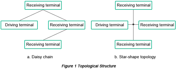
Topological structure of routing refers to routing sequence and structure of a signal line. In practical circuits, there is always a situation in which a single driving source drives multiple loads and driving source and loads conform to the topology of structure. Different topological structures have obviously different influence on signals. Usually, two types of basic topological structures are applied in PCB routing, that is, daisy chain and start-shape topology, which is shown in Figure 1 below.

a. Daisy chain
Routing starts from driving terminal and arrives at each receiving terminal sequentially. If series resistor is applied to change signal properties, the position of series resistor should be closely near to driving terminal. In terms of higher harmonic interference control, daisy chain features the best routing effect. However, this type of routing features the lowest routability, less than 100%. In practical designs, branch length in daisy chain should be short as much as possible. Routing space of this topological structure is small and a single resistor can be applied for compatibility with termination. Moreover, this type of routing structure makes signal receiving out of syne at different signal receiving terminals.
b. Star-shape topology
This type of routing is capable of effectively avoiding nonsynchronization of clock signals but it features a disadvantage that a terminal resistor is required by each branch. Resistance value of terminal resistor should be compatible with in-line characteristic impedance. For systems whose different signals have simultaneous requirement at receiving terminal, star-shape topology is the most suitable.
• Termination methods
Characteristic impedance on signal transmission path should be maintained constant, that is, reflection coefficient is 0, which means no reflection on transmission path. This situation is called impedance compatibility. At this time, signals transmit idea ground to terminal. Commonly, transmission line length should be compatible with condition  .
.
In this inequation, L refers to the length of transmission line; tr refers to the rising time of source terminal signals; tpd1 refers to load transmission delay at each unit length on transmission lines. When the integrated level transfer takes place prior to reflection arriving at far terminal, terminal matching technology is required to be applied. Terminal connection principles of transmission lines include: if either load reflection coefficient or source reflection coefficient is zero, reflection will be eliminated. Commonly, two strategies are applied: source impedance is made compatible with transmission line impedance, that is, source termination while load impedance is made to be compatible with transmission line impedance, that is, end termination.
1). Source termination
Source termination is mainly series termination method implemented by plugging a series resistor in transmission lines at positions adjacent to near-source end. The sum of resistance value of series resistor and driving terminal should be equal to resistance value of transmission lines. The principle of series termination is the elimination of reflected voltage from load terminal is to stop the second reflection of transmission lines, which is shown in Figure 2.

2). End termination
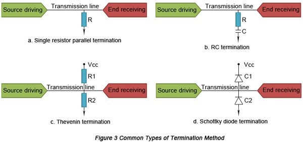
The main principle of end termination lies in pull-up or pull-down resistor adding to positions adjacent load terminal in order to implement impedance matching. End termination can be commonly divided into single resistor parallel termination, RC termination, Thevenin termination and Schottky diode termination, as is shown in Figure 3.

Resistance value in single resistor parallel termination is equal to the impedance of transmission lines. Values of two resistors in Thevenin termination should follow the formula: Z0=R1R2/(R1+R2). Value of capacitance in RC termination follows the formula: C=3T/Z0 in which T refers to the rising time of signals while Z0 refers to the impedance of transmission lines.
From the perspective of system design, parallel termination should be first picked up because it is the most capable of decreasing noise, EMI and RFI compared with other three termination methods. According to practical circumstances, the suitable termination method is picked up and when necessary, simulation design should be implemented.
Conclusion
In high-speed PCB design, successful prerequisites include reasonable layout and routing, avoidance of unnecessary turns and through vias, impedance continuity, integrated signal reference planes and excellent grounding. To optimize design & signal integrity and obtain higher electromagnetic compatibility, design simulation verification should be implemented. It helps designers deal with design defects in time and make up for shortcomings in PCB design.
Helpful Resources
• High-Speed Layout Tips
• High-Speed PCB Design Challenges on Signal Integrity and Their Solutions
• Signal Integrity Analysis and PCB Design on High-Speed Digital-Analog Mixed Circuit
• Full Feature PCB Manufacturing Service from PCBCart - Multiple Value-added options
• Advanced PCB Assembly Service from PCBCart - Start from 1 piece


 .
.

 .
.


