


In today's world of electronics manufacturing, where precision and efficiency are paramount, Printed Circuit Boards or PCBs form the core of each electronic product. The assembly of such PCBs requires great attention to detail so as to deliver functionality and reliability to electronic parts. One of the most vital tools in accomplishing this is the PCB stencil, particularly in the case of Surface Mount Technology or SMT assembly. Made primarily from materials like nickel or stainless steel, PCB stencils make it possible to apply solder paste accurately, and this is key to placing components on the board. Stencils, and why and how they affect good manufacturing processes in PCB assembly, are issues explored in this article.
Importances of Stencils
The Significance of Maintaining Accuracy and Uniformity of Solder Paste Deposition
The building block for quality PCB assembly is based on uniform and accurate solder paste deposition. PCB stencils are constructed with precisely aligned apertures that exactly fit the pads on the PCB. This ensures that solder paste is deposited only where components will reside, providing a foundation for robust solder joints. This degree of accuracy is important because it prevents common assembly defects like bridging, tombstoning, and poor solder joints—issues that can seriously degrade the electrical performance and lifespan of the end product.
Surface Mount Technology makes it much harder to achieve this accuracy since the components are tiny and positioned near together on the PCB. Here, monitoring the amount of solder paste is crucial to preventing flaws that might compromise the entire device by causing short circuits or bad connections.

Enhancing Production Efficiency
Stencils are a prime facilitator of the improvement in production efficiency by automating the solder paste application process. Earlier, this was carried out manually, and it was a slow, labor-intensive process with high human error. In contrast, stencils facilitate this process to be automated, significantly reducing the time to prep each PCB. This efficiency is particularly crucial in high-volume production environments, where rate and throughput are key competitive differentiators.
By using automated stencil print machines, the manufacturers can repeatedly apply paste onto large batches of PCBs speedily and reliably. Apart from enhancing productivity, this automation also reduces the cost of labor and material wastage associated with it, given the expectation from industry to conserve costs.
Reduction of Defects and Improved Reliability
Carefully designed, a stencil minimizes assembly errors, improving the reliability of electronic hardware. All of the design parameters of the stencil, such as thickness, shape, and aperture size, matter. These control the amount of solder paste deposited onto each pad. An excessive amount of paste will yield defects like solder balling and solder bridging, while inadequate paste will yield low-quality connections. Proper design and manufacturing of stencils are thus the key to achieving strong and sound solder joints.
Moreover, material selection for stencils has direct implications on the efficiency of release of paste. Suitable material having smooth aperture walls, such as electropolished stainless steel, enables better transfer of paste to lead to good transfer efficiency as well as dependable solder joint creation.
Types of PCB Stencils
Awareness of types of PCB stencils will help choose a suitable solution based on specific requirements of assembly. The main categories are illustrated below:
Framed Stencils: These are stencils that are mounted on a rigid frame to provide better support and stability for the application phase. They are exceptionally suited in working with more complex or larger-sized PCBs where utmost accuracy is considered. Despite their higher cost and extra room for storage requirements, they provide higher accuracy with the employment of automated equipment.
Step Stencils: Available in various thicknesses and levels of aperture, step stencils allow for differential solder paste depositing onto different portions of a PCB. This aspect is particularly useful with boards having various-sized and-pitched components. Step stencils are more costly and time-consuming to produce but are invaluable for some complex assembly processes.
Frameless Stencils: Without frames, these stencils provide flexibility and lower costs for smaller or simpler PCBs. They are easier to store and ship but might be troublesome for alignment during the process of applying the paste and therefore are not best suited for automated high-volume production.
Choosing the Proper PCB Stencil
The proper stencil is chosen based on a number of factors in order to provide optimal PCB assembly:
PCB Size and Complexity: Complex and larger boards may require the stability of framed stencils, whereas smaller and simpler boards may be acceptable with frameless ones.
Aperture Design and Size: For perfect paste deposition, apertures must be the same size and shape as component pads.
Material and Construction: Stainless steel and nickel are recommended because to their long life and precision, and the stencil's construction influences its efficiency and lifespan.
Features of Solder Paste: The stencil must be capable of supporting the physical properties of solder paste, e.g., particle size and viscosity.
Production Volume: Framed stencils can be compatible with high-volume runs due to their strength, whereas low-volume or prototype runs can utilize the cost-effectiveness of frameless designs.
Economic and Production Benefits
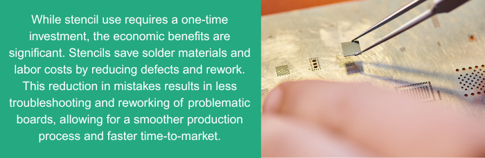
While stencil use requires a one-time investment, the economic benefits are significant. Stencils save solder materials and labor costs by reducing defects and rework. This reduction in mistakes results in less troubleshooting and reworking of problematic boards, allowing for a smoother production process and faster time-to-market. These economies are critical in today's competitive market for sustaining profit margins and product reliability.
Technological Advancements in Stencil Fabrication
Advanced manufacturing processes such as laser cutting, chemical etching, and electroforming have revolutionized stencil fabrication:
Laser Cutting: Offers precise, clean cuts, allowing complex and detailed designs with close tolerances.
Chemical Etching: Though less precise, it is cost-effective in large-volume manufacturing where ultimate precision is not crucial.
Electroforming: Delivers excellent release properties of the paste, being well-suited to fine-pitch applications due to its smooth trapezoidal sidewalls.
These technologies allow for custom design of stencils based on the specific needs of individual PCB designs in order to offer optimal performance.
Framework and Polishing Considerations
The stencil frame material, typically stainless steel, nickel, or aluminum, affects the usability and durability of the stencil. Different polishing methods, mechanical, chemical, and electropolishing, enhance aperture wall smoothness and solder paste release. Such optimizations reduce defects and enhance solder joint fidelity, which reinforces the reliability of the device.
PCB stencils are critical in achieving high-quality and efficient PCB assembly in the fast-evolving electronics industry. They offer precise and dependable solder paste depositing, without defects and rendering the PCBs more mechanically and electrically stronger. With the right selection of type and employing better design and manufacturing processes, the manufacturers are able to meet the strict specifications of modern-day electronics, presenting robust solutions that stay abreast of the times. At PCBCart, we comprehend these fundamental requirements and take efforts to support your assembly processes with highly engineered stencils that enhance productivity quality and efficiency. Contact PCBCart today to learn more on how our stencils may help improve your PCB assembly operation and obtain a quote that works for your specific needs. Let us help you become the best at your production work.


