Development of modern scientific technology leads to the increasing miniature of electronic components and massive application of SMT technology and devices in electronic products. SMT manufacturing device has attributes of full auto, high precision and high speed. Because degree of automation rises, higher requirements are brought to PCB design. PCB design must cater to SMT device requirements, otherwise manufacturing efficiency and quality will be influenced or even computer automatic SMT possibly fails to be completed. For example, the machine will possibly frequently break down when MARK isn't fully met; unreasonable design in terms of PCB shape, clamping edge and panel will influence manufacturing efficiency and pad defects or even machinery manufacturing can't be completed.
SMT, short for surface mount technology, is a type of advanced electronic manufacturing technology that solders and mounts components on the prescribed place of PCB. Compared with traditional THT (through hole technology), the most significant feature of SMT is the increased degree of automatic manufacturing that is fit for massive automatic manufacturing.
A basic integrated SMT production line should contain loader, printer, chip mounter, reflow oven and unloader. PCB starts from loader, transmitted along pathway and passing equipment with production completed. Then PCB will receive high-temperature soldering through reflow oven and be transmitted to unloader with manufacturing of printing, mounting and soldering completed. This process can be displayed in Figure 1 below.

PCB design is the key link contained in SMT technology, an important element determining SMT manufacturing quality. This article will analyze PCB design elements influencing its quality from the perspective of SMT equipment manufacturing. PCB design requirements from SMT manufacturing devices mainly include: PCB pattern, size, location hole, clamping edge, MARK, panel ways etc.
• PCB pattern
In the automatic SMT production line, PCB production starts from loader and completes production after printing, chip mounting, soldering. Finally, it will be generated from unloader as a finished board. In this process, PCB is transmitted on the pathway of device, which requires that PCB pattern should be in accordance with pathway transmission between devices.
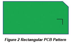
Figure 2 shows the standard rectangular PCB whose pathway clamping edge is as flat as a line so that this type of PCB is suitable for pathway transmission. Sometimes right angle is designed into chamfer.

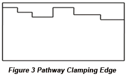
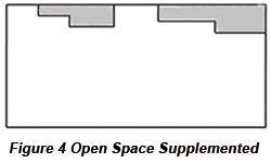
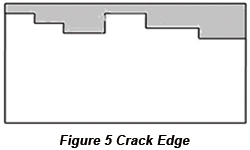
For the PCB design in Figure 3, its pathway clamping edge isn't a straight line so that both PCB location and transmission in device will be influenced. The open space in Figure 3 can be supplemented to make its clamping edge be a straight line as in Figure 4. Another method is to add crack edge to PCB, which is shown in Figure 5.


• PCB Size
PCB design size has to conform to the maximum and minimum size requirements of printer and chip mounter. Up to now, the size of most devices is in the range from 50mmx50mm to 330mmx250mm (or 410mmx360mm).
If the thickness of PCB is too thin, its design size shouldn't be too big. Otherwise, PCB deformation will be caused by reflow temperature. It's ideal that length-to-width ratio is 3:2 or 4:3.
If PCB size is less than the minimum size requirement of equipment, panelization should be carried out. The number of panels is determined according to PCB size and thickness.
• PCB location hole
SMT location methods are divided into two types: location hole together with edge location and edge location. However, the location method applied in our company is Fiducial Mark.
• PCB clamping edge
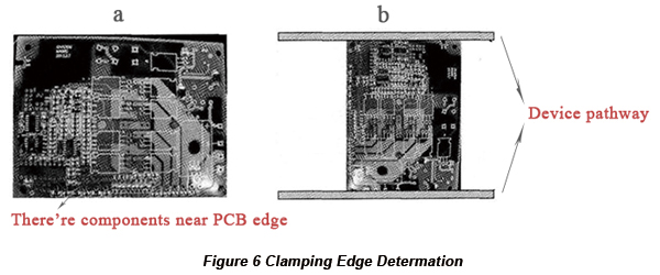
Since PCB is transmitted on the pathway of device, components mustn't be placed along the direction of clamping edge, or components will be pressed by device, influencing chip mounting. Take the PCB in Figure 6(a) for example, some components are placed near the lower edge of the PCB, so the upper and lower edges mustn't be taken as clamping edges. However, there are no components near the two side edges, so the two short edges can be used as clamping edges, which is shown in Figure 6(b).

• Mark
PCB Mark is identification point for all full-automatic devices' identification and location used to modify PCB manufacturing error.
a. Shape: solid circle, square, triangle, rhombus, cross, hollow circle, oval etc. Solid circle is the first choice.
b. Size: the size has to be in the range from 0.5mm to 3mm. Solid circle with diameter of 1mm is the first choice.
c. Surface: its surface is the same as soldering plane of PCB pad with soldering plane being even, neither too thick nor too thin and excellent reflector effect.
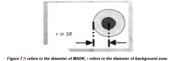
A background zone should be arranged around Mark and other pads, silkscreen and solder mask can't be contained in the background zone, which is shown in Figure 7.

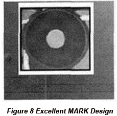
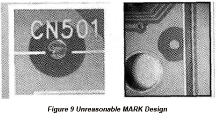
Figure 8 displays an excellent MARK design method while Figure 9 displays some MARK designs that are unreasonable.


Silkscreen characters and silkscreen lines are arranged around MARK in Figure 9, which will influence the device's identification of MARK and will lead to frequent alarm by MARK identification with manufacturing efficiency badly influenced.
• Panel method
In order to increase manufacturing efficiency, multiple small PCBs with the same or different shapes can be combined to form a panel. For some PCBs with double sides, top side and bottom side can be designed into one panel, which will produce a stencil so that cost can be reduced. This method also helps to reduce shift time for top side and bottom side, increasing manufacturing efficiency and device utilization.
The connection method of panels includes stamp hole and V groove, which are shown in Figure 10.

One requirement of V-groove connection method is to maintain the rest part of the board (uncut) equal to one fourth to one third of the thickness of the board. If too much of the board is cut off, the cut groove will possibly break down by the high temperature of reflow, leading to the falling of PCB that will be burnt in the reflow oven.
PCB design is such a complex technology that both device requirements and components layout, pad design and circuit design must be taken into consideration. Excellent PCB design is the significant element ensuring product quality. This article brings about some problems the PCB design should consider from the perspective of SMT manufacturing. As long as sufficient attention is paid to these problems, full automatic SMT manufacturing of SMT device can be carried out.


