In order to correct the errors generated in the process of PCB fabrication, Mark refers to a set of patterns used for optical localization. Mark can be classified into PCB Mark and local Mark.
PCB successfully added to your shopping cart


 English
 English
 English
 Español
 Deutsch
 Français
 Italiano
 日本語
日本語
 ภาษาไทย
 Malay
Malay
In order to correct the errors generated in the process of PCB fabrication, Mark refers to a set of patterns used for optical localization. Mark can be classified into PCB Mark and local Mark.
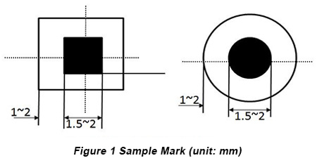
The shape and size of Mark should be designed according to the specific requirement of mounters with different models. Figure 1 is a sample of Mark, and the following table shows general requirements of Mark.

| Shape | Solid circle (●, optimal choice), triangle (▲), rhombus (◆), square (■), cross (+), hollow circle (○) |
|---|---|
| Size | The diameter is in the range from 1.5-2mm. The mark of mini-version and layout with high density can be shrinked but the diameter should be 0.5mm at least and the maximum diameter is over 5mm. |
| Surface | Bare copper, tin plating, gold plating (plating layer has to be flat and not too thick) |
| Surrounding | Considering the contrast between soldermask material color & environment, an area (1~2mm) without soldermask is around Mark. |
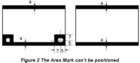
The layout position of Mark is determined by PCB transmission way of mounter. When lead rail is used to transmit PCB, Mark shouldn't be placed near clamping side or position holes and the specific size is different according to mounters. The general requirement is displayed in Figure 2 below.

• In the process of needle location, Mark can't be positioned.
• In the process of edge location, Mark can't be positioned within the area of 4mm from clamping side to edge.
PCB Mark is a set of patterns for optical localization of the whole PCB.

• PCB Mark position should be placed along diagonal line and the distance between them should be as large as possible.
• For PCB whose length is less than 200mm, at least 2 Marks should be placed like Figure 3a. For PCB whose length is more than 200mm, 4 Marks are required to be placed on PCB like Figure 3b and 1 or 2 Marks should be placed along or near the center line across the long side of PCB.
• Mark of panel should be placed along the diagonal line of each small board, which is shown in Figure 3c.
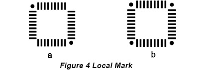
Local Mark refers to a set of patterns for optical localization of each component with many pins and small spacing between pins (distance between pins and center is no more than 0.65mm).

Local Mark position should meet the following requirements: For QFP components with more than 100 pins, 2 Marks should be placed along diagonal line as shown in Figure 4a. For QFP components with more than 160 pins, 4 Marks should be placed at the four corners as displayed in Figure 4b.
Whether you are looking for SMT PCB fabrication or SMT PCB Assembly service, PCBCart has the solution to make that happen. Even better, at very fair price! You are welcomed to use below PCB calculators to get your PCB prices. If you have any question on our capabilities or prefer discussing with us before ordering, we are available here.
Quote for FR4 PCBs Fabrication Online
Request FREE PCB Assembly Quote
Helpful Resources
• Influence on Printing Quality of PCB Based on Bad Design of Fiducial Marks
• Design Requirement of SMT PCBs Part One: Bonding Pad Design of Some Ordinary Components
• Design Requirement of SMT PCBs Part Two: Settings of Pad-Trace Connection, Thru-Holes, Test Point, Solder Mask and Silkscreen
• Design Requirement of SMT PCBs Part Three: Component Layout Design
• Full Feature PCB Manufacturing Service from PCBCart - Multiple Value-added options
• Advanced PCB Assembly Service from PCBCart - Start from 1 piece
Previous articleCommonly Seen PCB Design Issues
Next articleDesign Requirement of SMT PCBs Part Three: Component Layout Design
 PCBCart specializes in high-complexity, precision PCB assembly for mixed-volume batches, offering full-service electronic manufacturing excellence since 2005.
 [email protected] [email protected]
Thanks for your support! We'll go over your feedback in detail to optimize our service. Once your suggestion is picked up as the most valuable, we'll instantly contact you in email with a $100 coupon contained.