As an important carrier of all kinds of electronic components, printed circuit boards provide excellent mechanical support for components and connect those components through copper foil lines with different thickness and soldering pads with different sizes according to logical circuits to implement the electric performance of products. Since most electronic products are manufactured by SMT, the quality of PCB design is both directly related with the normal operation of electric performance and with the effective operation of PCB assembly manufacturing. With the influence of Fiducial Mark on printing quality, this article discusses the important influence of PCB manufacturability in the field of electronic product manufacturing in point-to-area method.
Functions of Fiducial Marks
In the process of volume production of electronic products with the method of SMT devices, each batch of PCBs for assembly has to conform to the requirements of correct board and accurate position. Manual operation without special design can lead to low efficiency and accuracy, which will possibly cause the defects of products.
The accurate positions of board can be generally ensured through positioning holes or Fiducial Marks. Since the design of positioning holes relies on brand and model number of PCB assembly equipment, positioning holes are not placed on each PCB while Fiducial Mark is the necessity of each PCB.
Fiducial Mark is a special optical positioning symbol. During manufacturing, assembly devices irradiate on Fiducial Mark with image coordinates generated which are then compared with the preset standard data in the system. If coordinates are compatible with standard data or the differences are within allowed category, the machine will judge the correctness of PCBs that will be sent to the inside of machines for procedures including printing, mounting and soldering. Otherwise, PCBs will be judged with incorrectness and board sending will be paused with alarm transmitted.
Therefore, Fiducial Mark plays a significant role in correctness of electronic products guarantee. Nevertheless, many PCB designers sometimes fail to make their designed PCBs not recognized by assembly devices so that the subsequent normal production can't be implemented. It's extremely necessary to be aware of the requirements and regulations of Fiducial Mark in the process of PCB design.
Requirements of Fiducial Mark Design
• Composition of Fiducial Mark and design parameters
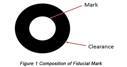
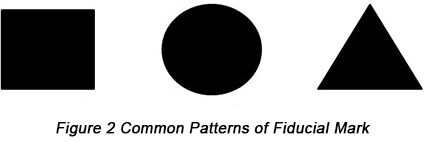
An integrated Fiducial Mark contains mark and clearance, which is displayed in Figure 1. The general patterns of Fiducial Mark are shown in Figure 2.


Generally speaking, the solid circle with a diameter of 1mm (±0.2mm) is the optimal choice for Fiducial Mark that is made of bare copper, tin plating or nickel plating protected by transparent inoxidizable coating. In order to make Fiducial Marks easily recognized by assembly devices, the color of Fiducial Marks should be obviously different from that of surrounding area. Besides, clearance with the size 1mm larger should be set aside Fiducial Marks. Generally, the radius of clearance is no less than 2R (R refers to the radius of Fiducial Mark) and when the radius of clearance is equal to 3R, the recognition effect of devices is the best.
• Routing requirements of Fiducial Marks
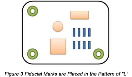
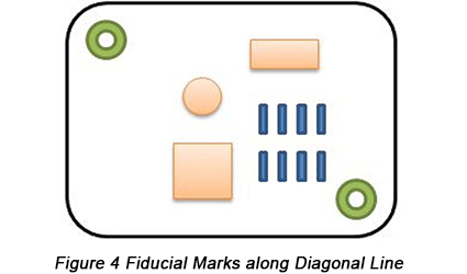
Based on the theory that 3 non-linear points determine a plane, 3 Fiducial Marks should be placed with a pattern of "L" on the PCB as shown in Figure 3. If the space of the board is limited so that 3 Fiducial Marks can't be placed on it, at least a pair of Fiducial Marks should be placed on the board along diagonal line, just like Figure 4.


Fiducial Marks along diagonal line should not be placed completely symmetrically. Otherwise, error can't be found out by devices when boards are not correct so that defects will come up with inaccurate board or incorrect mounting. For components with some special requirements and accurate positioning, local Fiducial Marks can be designed to increase the accuracy of mounting.
In addition, the distance between Fiducial Marks and PCB edge has to be bigger than the minimum distance requirement clamped by SMT devices, to be within PCB instead of at the board edge and to meet the clearance requirement of the minimum Fiducial Mark. Besides, in order to increase the recognition effect of printing device and mounting device, other routing, silkscreen, soldering pad or V-Cut shouldn't be set within Fiducial Mark clearance and the distance between clearance and other metal points (test point for example) with similar types has to be 5.0mm at least.
• Manufacturing requirements of Fiducial Marks
In the process of bare board PCB manufacturing, the size change from Fiducial Marks has to be no more than 25μm. If the size change is too big, the data deviation acquired by computer image will exceed the change category of standard values so that both board loader and alarm will be influenced and the manufacturing efficiency will be downsized.
The surface flatness of Fiducial Marks should be controlled within 15μm and they have to share the same inner background. Otherwise, the low degree of flatness will possibly influence the recognition effect of devices or devices even wouldn't work.
All the Fiducial Marks on the PCBs with the same board number have to be the same in terms of size and shape. It is suggested that all the Fiducial Marks be marked as solid circles with diameter of 1mm. The best performance can be obtained when high contrast comes up between Fiducial Marks and substrate material of PCBs. In addition, Fiducial Marks should be isolated with copper foil on copper foil boards.
Case Analysis
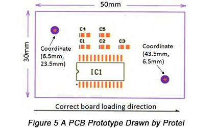
In order to provide an easy-to-understand explanation, a PCB prototype with the size 50mmx30mm is drawn by Protel software with its Fiducial Marks placed along diagonal line as shown in Figure 5.

For the Fiducial Marks design in Figure 5, the device is capable of recognizing and comparing parameters by camera with the correct board loading direction to ensure the correct printing work done by printer.
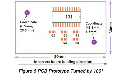
However, once the board loading direction is incorrect such as the situation shown in Figure 6 in which the prototype is overturned 180°, device will still stick to the correctness of board loading direction and positions of the present PCB. Under this condition, normal printing work will be implemented according to established procedure.

This will greatly reduce the manufacturing efficiency. What's worse, since the efficiency of PCBA is quite high, a lot of problematic PCBs will be generated prior to the pause of manufacturing after advent of defected PCBs. In this circumstance, manufacturing time and efficiency will be decreased and product quality will be even influenced.
Aside from the placement of Fiducial Marks that they should avoid complete symmetry, the distance between Fiducial Mark edge and board edge should also be noticed. The distance should be set in the range from 3.5mm to 5mm. In addition, the mark of Fiducial Marks has to be medium, neither too big nor too small. For circle pattern, the diameter should be controlled in the range from 1.0-3.0mm. If the diameter is too big, the device will make a relatively large place adjustment so that relatively large deviation will take place with printing defects. If the diameter is too small, the device will possibly fail to recognize them so that the device will refuse to load boards or make alarm.
In conclusion, although it is relatively simple to design Fiducial Marks, some details tend to be neglected. If they are designed improperly, the corresponding functions Fiducial Marks should have can't be implemented and even some problems will possibly take place, leading to printing errors and delayed manufacturing. Therefore, circuit designers must master the theoretical knowledge on circuit design, and the requirement of assembly device on PCB manufacturing and they have to consider all the requirements listed from all aspects of production line to increase the manufacturability, manufacturing efficiency and economy of products.
Helpful Resources
• Design Requirement of SMT PCBs Part Four: Mark
• Full Feature PCB Manufacturing Service from PCBCart - Multiple Value-added options
• Advanced PCB Assembly Service from PCBCart - Start from 1 piece


