


PCB successfully added to your shopping cart
Design Requirement of SMT PCBs Part One: Bonding Pad Design of Some Ordinary Components
The size design of rectangular SMC or SMD is shown in Figure 1 below.

Rectangular SMC (surface mount component) or SMD (surface mount devices)
The size design of rectangular SMC or SMD is shown in Figure 1 below.

The groove depth of the rub groove bonding pad is calculated based on formula (unit: mm): 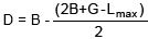
Note: Lmax refers to the maximum length of component shell; B refers to the length of bonding pad pattern; G refers to the distance between two bonding pad patterns; D refers to the depth of rub groove bonding pad; C refers to the width of rub groove bonding pad whose value is generally set as 0.3±0.05mm.
SOT (small outline transistor)
Design requirement of single pin bonding pad is shown in Figure 3.

For SOTs, center to center distance between bonding pads should be the same as that between leads and the size adjacent to each bonding pad should be expanded by at least 0.35mm, which is displayed in Figure 4.

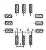
SOP and QFP Components
Since the pins of SOP and QFP are all wing shaped, the size of bonding pads is calculated in the same method. Generally speaking, the width of bonding pad is half the center to center distance of adjacent pin and the value of the length of bonding pad is 2.5±0.5mm.
The shape of SOP and bonding pad design are shown in Figure 5 below.

• The center to center distance between bonding pads is the same as that between pins.
• The general principle of bonding pad design for single pin is:
- a. W2≤W when distance between pins of components is no more than 1.0mm;
- b. W2≥ 1.2W when distance between pins of components is no less than 1.27mm.
- c. L2 = L + b1 + b2; b1 = b2 = 0.3-0.5mm.
• The distance between two parallel bonding pads is calculated based on formula (unit: mm): G = F - K.
Note: G is the distance between 2 bonding pads; F is the package size of component shell; K is the constant whose value usually set as 0.25mm.
• The shells of SOPs are usually divided into two types: wide body and narrow body. The value of G is 7.6mm and 3.6mm respectively.
The size of QFP bonding pad and solder mask is listed in below table:
| Number of leads | Bonding pad size | Soldermask size | Configured legend | |||
|---|---|---|---|---|---|---|
| a | b | c | d | e | ||
| 64 | 1.0 | 0.6 | 0.18 | 0.2 | 0.135 |
 |
| 80 | 0.8 | 0.5 | 0.2 | 0.13 | 0.085 | |
| 100, 160 | 0.65 | 0.35 | 0.3 | 0.13 | 0.085 | |
| 48, 208 | 0.5 | 0.3 | 0.3 | 0.1 | 0.05 | |
| 224 | 0.4 | 0.22 | 0.22 | 0.08 | 0.05 | |
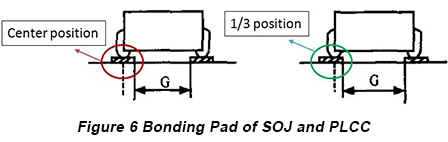
SOJ and PLCC
• Pins of SOJ and PLCC are J shaped with typical center to center distance between pins at 1.27mm and same bonding pads pattern.
• Bonding pad design
a. The width of bonding pad for single pin is generally in the range from 0.50-0.80mm while the length of bonding pad from 1.85-2.15mm.
b. The center of pins should be between one third inside of bonding pad shape and center of bonding pad, as is shown in Figure 6.
c. The distance between two parallel bonding pads of SOJ (G) is generally 4.9mm.
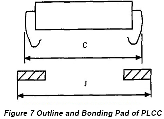
d. The distance between two parallel bonding pads of PLCC is calculated based on the following formula J = C + K as shown in Figure 7.
Note: J refers to the outlined distance of bonding pad shape; C refers to the maximum package size of PLCC; K refers to the constant whose value is generally set as 0.75mm.
BGA (ball grid array)
• Classification and attributes of BGA
a. BGA refers to the package type in which ball grid array is set as I/O leading out terminal at the bottom of components. It can be classified into the following types: PBGA (plastic ball grid array), CBGA (ceramic ball grid array), TBGA (tape ball grid array) and μBGA (chip scale package BGA). The outline size of BGA is in the range from 7-50mm.
b. PBGA is the most prevalent BGA package type with PCB substrate as a carrier. The spacing between solder balls of PBGA is 1.50mm, 1.27mm and 1.0mm while the diameter of solder balls can be 1.27mm, 1.0mm, 0.89mm and 0.762mm.
c. The solder balls at the bottom of BGA have two types of distribution: incomplete distribution and complete distribution, which is shown in Figure 8.

• Design principle of BGA bonding pad
a. Design is carried out according to BGA bottom solder balls distribution. It is required that each center of each solder ball is compatible with solder ball center of the corresponding solder ball at the bottom of BGA component.
b. The bond shape of each solder ball is solid circle and the max diameter of PCB pad is the same as the pad diameter of solder balls at the bottom of BGA components. However, the min diameter of PCB pad is obtained by pad diameter at the bottom of BGA component minus mount accuracy. e.g., if pad diameter at the bottom of BGA is 0.89mm and mount accuracy is 0.1mm or so, the min diameter of PCB pad is in the range from 0.89-0.2mm.
c. The size of solder mask should be larger than that of bonding pad by 0.1-0.15mm.
d. Through holes have to be blocked by dielectric material or conducting gel after electroplating and its height has to be no more than the height of pad.
e. Silkscreen pattern should be generated at the 4 angles from side corridor of BGA component and the line width of silkscreen is between 0.2-0.25mm.
Got SMT PCB Production Requirements? Reach PCBCart for a free SMT PCB Quote Today!
PCBCart has been manufacturing SMT PCBs for worldwide companies of all sizes since our establishment in 2005. We are known for our quality pcb fabrication & assembly expertise and constant professional support. We are proud of our 99%+ customer satisfication rate! Reach us for a free and no-obligation quotation for your SMT PCB project today!
Get an Instant Quote for FR4 PCBs
Helpful Resources
• Elements Ensuring Excellent PCB Pad Design for QFN
• Design Requirement of SMT PCBs Part Two: Settings of Pad-Trace Connection, Thru-Holes, Test Point, Solder Mask and Silkscreen
• Design Requirement of SMT PCBs Part Three: Component Layout Design
• Design Requirement of SMT PCBs Part Four: Mark
• Full Feature PCB Manufacturing Service from PCBCart - Multiple Value-added options
• Advanced PCB Assembly Service from PCBCart - Start from 1 piece