As a platform for numerous components and circuit signal transmission, Printed Circuit Boards (PCBs) have been regarded as such a key section of electronic information products that their quality determines quality and reliability of end products. Owing to uprising development trend towards high density and lead-free and halogen-free environmental requirement, if professional and timely inspection leaves undone, all kinds of failure issues possibly take place to PCBs such as bad wettability, crack, delamination etc.
In order to ensure both high quality and reliability of assembled PCBs, PCB manufacturers and assemblers have to implement inspections for boards at different stages during manufacturing and assembly procedure so that surface defects will be eliminated. Furthermore, timely and professional inspections are capable of leading defects to be exposed prior to electrical test and are beneficial for data accumulation for Statistical Process Control (SPC). Wide application of Surface Mount Technology (SMT) raises higher requirement for inspection because SMT solder joints have to withstand more stress than those with the application of Plated-Through-Hole (PTH) technology. Since device leads depending on SMT have to stand more structural load, devices won't be firmly soldered onto the board without sufficient solder. Therefore, long-term electrical reliability of circuit boards with surface mount devices assembled on dramatically depend on structural integrity of solder joints, which adds definite necessity to PCBA inspection.

Up to now, apart from visual inspection, multiple structural inspection technologies are available with different cost, performance and defect coverage. Automatic inspection technologies include optical inspection, laser triangle measurement, X-ray inspection and X-ray lamination technology. To implement optimal process inspection, manufacturers should be aware of both advantages and disadvantages of each type of inspection method and make clear where each type performs best. In general, PCB assembly inspection technologies are classified into two types: visual inspection and automatic process inspection.
a.Visual Inspection
Visual inspection can be used after lots of steps during PCB assembly process and equipment for visual inspection is selected based on the positions of inspection targets. For example, after solder paste printing and device placement, inspection staff is able to find out obvious defects with naked eyes such as contaminative solder paste and missing components. The most prevalent visual inspection is capable of inspecting reflow solder joints by observing light rays reflected from ordinary prism from different angles. Generally speaking, this type of inspection can test 5 joints in just one second.
Validity of visual inspection depends on inspection staff's capability, consistency and applicability of inspection standard. Inspectors have to be fully aware of technical requirement for each type of solder joints since each type of solder joints possibly contain as many as eight kinds of defect standards while over 6 types of solder joints are possibly available on different assembly devices. Thus, it's inapplicable for visual inspection to be used in quantitative measurement for effective structural process control. Moreover, visual inspection isn't fit for hidden solder joint inspection such as those on J-lead devices with high density package, ultramicro fine square flat devices, surface array flip chip or BGA (ball grid array) devices. Based on uniform and specific rules establishment, visual inspection is regarded as a technology with low cost and easy access, applicable for large defect inspection.
b. Structural Process Test System (SPTS)
Digitalization and analysis system of real-time and automatic video capture is capable of dramatically improving allowance and repeatability of visual inspection. Therefore, structural process test system depends on some form of emitting light like visible light, laser beam and X ray. All those systems acquire information through processing images to find out and measure defects concerned with solder joint quality. Similar with visual inspection, SPTS is implemented without the need to physically contact circuit board. Different from visual inspection, however, SPTS features such high repeatability and eliminates subjectivity from defect measurement.
• Automatic/Automated Optical Inspection (AOI)
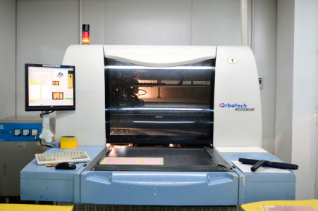
AOI system relies on multiple light sources, programmable LED library and some cameras to shine solder joints and take shots. Under reflected light, leads and solder joints play a role as mirror reflecting majority of light while both PCBs and SMDs reflect little light. Light reflected from solder joints fails to provide the practical height data while graphics and intensity of reflected light provides information in terms of solder joint curvature. Then professional analysis will take place to determine whether solder joints are complete, whether solder is sufficient, whether bad wetting takes place. Apart from that, AOI system also inspect solder bridging and missing components or displacement before or after reflow soldering. AOI equipment runs at a speed of 30-50 joints per second and features relatively LOW cost. Nevertheless, it fails to inspect parameters of some solder joints such as weld height and solder in a joint and fails to inspect hidden solder joints such as those belonging to BGA, PGA and J-shape lead devices that are essential to reliability of soldering. In conclusion, AOI test performs BEST at inspection of ICs and gull-wing devices with pitch larger than 0.5mm.

• Automatic Laser Test (ALT) Measurement
ALT is a more direct technology used to test height and shape of solder joints or solder paste deposition. This system runs to measure the height and reflectivity of some surface components when the image of laser beam focuses on one or multiple position sensitive detectors that maintain a certain angle with laser beam. During ALT measurement, surface height is determined by the light position reflected from position sensitive detectors while surface reflectivity is figured out from the power of reflected light beam. Due to secondary reflection, light beam perhaps shines on position sensitive detectors at multiple positions, which calls for a scheme to distinguish correct measurement. Furthermore, reflected light beam may suffer from shielding or interference of interference material when running along light of position sensitive detectors. In order to eliminate multiple reflections and prevent shielding, this system should test reflected laser beam along regulated independent optical path. During multiple height measurement for solder joints, ALT system is OPTIMAL for solder paste deposition quantity and position alignment prior to component assembly. It provides data for real-time structural process control of solder paste printing including viscosity, alignment, cleanliness, fluidity and squeezing speed and stress.
• X-ray Fluoroscopic System
X-ray fluoroscopic system emits a beam of rays from a single-point light source, which vertically goes through circuit board. With this process carrying on, solder joints weaken the intensity of rays to larger extent than other materials. The intensity changes on ray energy are converted into digital X-ray graphics with a gray scale of 256. Gray X-ray graphics of some solder joint is actually a density image indicating solder joint thickness, distribution and internal integrity. On a single-side PCB, X-ray fluoroscopic system is capable of accurately inspecting solder joint defects such as those (including crack, insufficient solder, bridging, misalignment, void etc.) taking place on J-shape wiring devices, gull-wing devices or passive chips. Apart from that, it is able to inspect missing components and reversed tantalum capacitors. When it comes to double-side PCBs, however, X-ray fluoroscopic system fails to accurately inspect those defects due to possible overlapping of X-ray images of solder joints on both sides of a board.
• X-ray Lamination System
Compared with X-ray fluoroscopic system, X-ray lamination system generates focal plane of a horizontal section area through scanning or synchronously spinning with X-ray detector. Off-axis images generated on detectors then lead to the generation of section image with surface thickness of 0.2-0.4mm by single swinging or multiple swinging that causes homogenization. Furthermore, components at front side and back side of focal plane become defocused in laminated images so that solder joints within focal plane are departed from other materials on PCBs. Depending on laser range finder, X-ray lamination system draws board surface position relative to focal plane and rectifies board warpage. After that, circuit board is moved at a small vertical increment so that it goes across focal plane, after which different sections of the same solder joint can be inspected. It works perfectly for BGA and PTH solder joint inspection. Double-sided PCB is vertically moved at large increment to go across focal plane to inspect solder joints at both sides of the board. Through modifying beam's scanning radius and vertically moving focal plane, different amplification factors or visual area sizes can be set. X-ray lamination system can measure parameters of all physical solder joints at different focal planes so that process defect coverage can be provided. Due to the indicated relationship between section image of X rays and given solder paste volume, grey scale readings can be converted into practical sizes by regulated standard units or metric units. After analysis on measurement results, data will be provided to characterization and assembly improvement. For example, average solder paste thickness or solder paste volume change of solder joints can lead people to be aware of quality levels of solder paste printing and defect sources. X-ray lamination system runs at an inspection speed of 30-40 joints per second. It ensures 100% coverage of key device inspection by running at a flexible sample way, but it fails to cover 100% of devices whose assembly period takes place in fewer than 45 seconds. X-ray lamination system features the highest cost among all inspection methods but greatly shortens time of searching and rework.
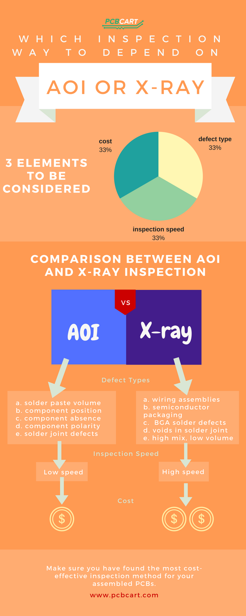
In spite of so many types of inspection methods, much doubt falls on difference between AOI inspection and X-ray inspection. The image below demonstrates inspection method determination elements and clarifies fields where AOI and X-ray inspection performs best.

Three elements should be taken into consideration when deciding inspection method: defect type, cost and inspection speed.
When it comes to defect types AOI and X ray cover, AOI is usually applied for inner layer test prior to lamination and defect items range from solder paste volume, component position, absence and polarity, to solder joint defects. The former, however, focuses on fine and micro defects after lamination and is capable of testing wiring assemblies, semiconductor packaging, BGA solder defects, voids in solder joint and high mix, low volume assembly.
For inspection speed, AOI inspection indicates a lower speed than X-ray inspection. Nevertheless, high speed and accuracy leads to higher cost.
Printed Circuit Board assembly manufacturing hardly relies on single inspection method. After all, visual inspection can never be avoided during assembly procedure. Due to complexity improvement and high volume assembly demand, automatic inspection methods have to be used. As a turnkey PCB assembler with over 20 years' experience, PCBCart is highly skilled at mounting electronic components onto circuit boards. To guarantee the quality, we launched a special department responsible for PCB inspection. Quotation is always free and quick - click the following button to submit your circuit spec and files. We will give PCBA price shortly.
Request Free PCB Assembly Quote
Helpful Resources
• Automated X-ray Inspection Technology Introduction
• Automated Optical Inspection Technology Introduction
• Why is X-ray Inspection Technology So Important in PCB Assembly?
• PCBCart offers Bed of Nails Fixture Test and Flying Probe Test
• PCBCart Assembly Service Introduction and Capabilities


