X-ray inspection technology, usually referred to Automated X-ray inspection (AXI), is a technology used to inspect the hidden features of target objects or products with X-rays as its source. Nowadays, X-ray inspection is widely used in lots of applications such as medical, industrial control, and aerospace. As for PCB inspection, X-ray is massively used in the process of PCB assembly in order to test the quality of PCBs, which is one of the most important steps for quality-oriented PCB manufacturers.
Nothing can be loved blind. So this passage will tell you why X-ray inspection technology is so important in PCB assembly.
Technology Development Pushes X-ray Forward
In recent years, area array packages including BGAs and QFNs, flip chips and CSPs are widely used in all kinds of fields such as industrial control, communication, military industry, aerospace etc, making solder joints hidden under the packages. This fact makes it impossible for traditional inspection devices to play their role perfectly in PCB inspection. In addition, since the appearance of surface mount technology (SMT) that makes both packages and leads become smaller, traditional inspection methods including optical, ultrasonic and thermal imaging are insufficient because PCBs have higher density with their solder joints hidden and holes buried or blind. Besides, with the increasing miniaturization in terms of semiconductor components package, while considering X-ray inspection system, the trend of both present and future component miniaturization can' t be neglected. Compared with other inspection methods, X-ray is capable of penetrating into inner packaging and inspecting the quality of solder joints. That's why it is picked up.
Principles of X-ray Inspection
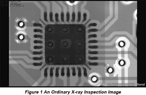
X-ray has a unique advantage that is materials absorb X-rays proportional to their atomic weight and all materials absorb the X-ray radiation differently depending on their density, atomic number and thickness. Generally speaking, materials made of heavier elements absorb more X-rays and are easily imaged, while materials made of lighter elements are more transparent to X-rays. Therefore, an ordinary X-ray inspection image is shown as Figure 1.

From this figure, the dark black image refers to the material made of heavy elements while the transparent or relatively white image refers to the material made of light elements. Therefore, X-ray inspection is good at inspecting hidden defects including opens, shorts, misaligned, electrical components missing and so on.
All the X-ray inspection devices are composed by the following three elements:
a. X-ray tube. It is capable of generating X-ray.
b. A sample operation platform. It is capable of moving with a sample in order to make the sample inspected from different angles and magnification adjusted. And oblique angle inspection can also be done.
c. A detector. It is capable of catching the X-ray through the sample and converting it into the image that can be understood by users.
The inspection principle of all X-ray inspection devices is X-ray projection microscope. The process starts with the generation of X-ray by X-ray launching tube passing through inspected PCBs. Since different materials have different X-ray absorption based on the differences in terms of material and atomic number. Projection is generated on detectors and the higher the density is, the deeper the shadow will be. The shadow will be largely close to X-ray tube and vice versa.
Therefore, the ideal X-ray inspection system must have clear X-ray images so as to provide the information in the process of defect analysis. For this goal, an X-ray inspection system must have sufficient magnification to meet the present and future needs. Besides, for the analysis of BGAs and CSPs, oblique angle inspection function must be available. Because without it, solder balls can only be inspected from right above so that the more detailed information for analysis would be lost concerning the size and thickness of solder balls.
Classification of X-ray Inspection Devices
X-ray inspection systems for BGAs and CSPs are mainly classified into two categories: 2D (two dimensional) system and 3D (three dimensional) system. All the devices can be operated off line and are capable of making panel inspection and sampling inspection. Off line devices make it convenient to inspect PCBs at any stage in the assembly line and easy to be back to the assembly line again. Some X-ray devices are used on-line so that most of these devices are put after reflow oven. Whether to use on-line or off-line devices relies on the application and inspection amount. Generally speaking, online devices are suitable for applications with large quantity, complexity and few type changes based on the extra cost and safety elements. However, on-line X-ray inspection systems are basically the slowest part in the assembly line, making fabrication line capacity become low. So even if in the application with high capacity, off-line devices can be used to make panel inspection with cost taken into consideration.
A 2D X-ray system is capable of displaying simultaneously the 2D images of all the components from both sides of PCB just like the medical application used to inspect the bone fracture conditions. A 3D X-ray system is capable of generating the images of cross sections by rebuilding a series of 2D images just like the medical application, CT. Besides its cross section inspection, 3D system has another method which is Laminography. The inspection process is carried out by combining the image of a cross section and eliminating the images from other cross sections to rebuild the image of a certain cross section. 2D systems can be operated on line or off line. So can X-ray laminography. However, the on line method usually costs more time. The X-ray inspection system with CT function is accomplished off line because many 2D images and complicated algorithm are needed so that a couple of minutes have to be cost. Therefore, X-ray inspection system in CT type is only used in the less important professional research analysis application. Other 2D and 3D systems must be instructed with a privilege of the least time and the best image so as to reduce the cost of inspection.
X-ray Tube is the Heart of X-ray Inspection Device
For all kinds of X-ray inspection devices, X-ray tube is the most essential part. Nowadays, X-ray tubes can be classified into two categories: open tube and closed tube. The feature comparison between the two types of tubes is shown in Table 1.
|
Feature
|
Open tube
|
Closed tube
|
| Min. resolution |
≤1μm |
≥μm |
| Max. tube voltage |
≥160KV |
100KV |
| Magnification |
High |
Low |
| Filament lifespan |
300-800 hours |
About 10,000 hours |
| System maintenance cost |
Filament/device maintenance;
pro vacuum pump is required
to pump vacuum. |
Not needed |
When choosing the type of X-ray tube, some elements must be taken into consideration:
a.X-ray tube type: open tube or closed tube. This type is correlated with the resolution and lifespan of inspection devices. The higher the resolution is, the more intricate and delicate details users will see. If the target inspected is at a large scale, then it won't matter when you choose the device with a relatively low resolution. However, as far as BGAs and CSPs are concerned, the resolution of 2μm or smaller is required.
b.Target type: penetrating or reflective. The target type plays a role in influencing the distance between the sample and X-ray tube focus that will eventually influence the magnifying times of inspection devices.
c.X-ray voltage and power. The penetration capability of X-ray tube is proportional to the voltage. When voltage is large, objects with higher density and thickness can be inspected. When the inspected target is single-sided boards, devices with low voltage can be chosen. However, when the inspected target is multi-layer boards, high voltage is required. As for the certain voltage, the image definition is proportional to X-ray tube power.
All in all, X-ray inspection technology has brought new reforms to SMT inspection methods, and it can be regarded as the best alternative for PCBA manufacturer to further increase the fabrication craft and product quality.
PCBCart offers X-ray inspection on our assembled circuit boards to test their quality. We promise to ship out only qualified boards. Interested in getting a quick quotation for your custom PCB Assembly project? Click the following button to submit RFQ. We will give the pcb assembly price and lead time within 1-2 working days.
Request for PCB Assembly Quotation with X-ray Inspection
Helpful Resources
• A Comprehensive Introduction of PCBA
• Printed Circuit Boards Assembly Process
• Design for Manufacture and Assembly of PCBs and General Rules it Conforms to
• How to Evaluate A PCB Manufacturer or A PCB Assembler
• 6 Effective Ways to Cut PCB Assembly Cost Without Sacrificing Quality


